Differences from a conventional diode
This component passes electric current in one direction and does not pass it in the other, like other classic diodes, but provides high speed and low voltage drop during transition.
The most important feature of the Schottky diode is that instead of the usual electron-hole junction, the principle of contact between metal and various semiconductor materials is used, which has a positive effect on increasing the operating frequency. Diffuse capacitance and the recombination process do not appear in the contact region, since there are no minority charge carriers in the so-called transition zone. The intrinsic capacity of this layer tends to 0.
Thus, these products are microwave diodes for various purposes:
- pulsed;
- avalanche-flight;
- mixing;
- detector;
- multiplying;
- parametric.
Another feature is that most Schottky diodes are low voltage and static sensitive models. However, it is wrong to perceive this as a categorical disadvantage, since this makes it possible to use these tools for processing low-power radio signals.
Finally, such products are more stable when applying electric current than other analogues, since crystal formations (silicon substrate) are embedded in their body.
Main characteristics of diodes
First, let's remember what a regular diode is and how it works. This is a semiconductor device that consists of two zones. Under certain conditions, electrons move through this transition.
Diode design and designation
The main property of the element is that it allows current to pass in one direction and not in the other. Schottky diodes have the same characteristics as conventional ones. Let’s focus on some in more detail. These are voltage drop, reverse current, reverse voltage, frequency.
How does a Schottky diode work?
The element structure includes several parts:
- epitaxial layer;
- substrate;
- security ring;
- metal film;
- barrier;
- external contact.
The base is usually made of silicon or gallium arsenide, but if the circuit needs to be highly resistant to temperature changes, germanium is used. The materials used for sputtering are palladium, silver, platinum, tungsten, aluminum or gold. It is noteworthy that the back side of the semiconductor is more heavily doped. The level of alloying and type of metal affect the rectification characteristics.
The operating principle is based on the characteristics of the barrier. In the semiconductor, in the contact region, a layer is formed that is significantly depleted of electrons, but has valve properties. Thus, a barrier for charge carriers appears.
Depending on the power, there are several types of Schottky diodes:
- small;
- average;
- high.
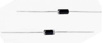
Based on the design features, there are types for surface or volumetric mounting, as well as modules and rectifier analogues. When choosing rectifier components, you should pay attention to the current and voltage indicators, as well as the material of construction and mounting method. There are also 3 variations of diode assemblies: models with a common anode, elements with doubling and three leads, as well as varieties that have a lead from a common cathode. For all types, there is a limit on the permissible reverse voltage of 1200 volts.
Design
The Schottky diode differs from ordinary diodes in its design, which uses a metal-semiconductor rather than a pn junction. It is clear that the properties here are different, which means the characteristics should also be different.
Indeed, a semiconductor metal has the following parameters:
- Leakage current is of great importance;
- Low voltage drop across the junction when connected directly;
- Restores charge very quickly, as it has a low value.
The Schottky diode is made of materials such as gallium arsenide, silicon; much less commonly, but can also be used, is germanium. The choice of material depends on the properties that need to be obtained, however, in any case, the maximum reverse voltage for which these semiconductors can be manufactured is not higher than 1200 volts - these are the highest voltage rectifiers. In practice, they are much more often used at lower voltages - 3, 5, 10 volts.
Application of Schottky diodes
The components are actively used as part of various devices and equipment:
- computer equipment and consumer electronics;
- power high-frequency rectifiers;
- solar panels and radiation receivers;
- radio and television equipment;
- audio amplifiers and MOSFETs;
- stabilizers and power supplies.
The products are used wherever a minimum forward voltage drop is required. Their popularity is due to the advantages of Schottky diodes, which make it possible to restore the reverse resistance of electric current, stabilize voltage, absorb radiation, and also increase the efficiency of final devices.
Despite the advantages, such devices have disadvantages. But there are only two of them:
- in the event of an increase in temperature, a significant increase in the reverse current is recorded;
- the breakdown is irreversible in cases of short-term excess of the critical voltage.
There are three main faults that can occur with diodes of this type: break, breakdown and leakage (the most difficult to identify). Diagnostics is carried out using a universal tester (multimeter). To obtain accurate results, the test will require soldering and measuring reverse resistance. When using a standard tester, the specified electric current value should be taken into account.
Application in electronics
Properties such as speed and low voltage drop allow the use of Schottky diodes in high-frequency circuits. For example, in high-frequency power rectifiers (up to hundreds of kilohertz), where they work as high-frequency rectifiers. They are also used in sound amplifiers, since compared to conventional diodes they produce a lower level of interference.
If you look at the power supply board, you will definitely see a Schottky diode
Another application is as an integral part of more complex semiconductor devices. For example, MOS transistors, diode assemblies and power diodes with a built-in Schottky diode have better characteristics.
The scope of application of the products is wide, but they are most often used in computer power supplies. And also in circuits for modulating light in radiation receivers and solar batteries.
How a Schottky diode is marked and indicated in diagrams
Often, a Schottky diode will be labeled as a regular diode on a schematic, and additional information about the type of component will be included in the specification sheet.
As a rule, the marking of Schottky diodes is a set of symbols printed on the product body in accordance with international standards. Depending on the country of origin, labeling may vary. In any case, you can decipher the code using radio engineering reference books.
If necessary, you can replace the standard diode with a similar device with a barrier - the main thing is that the current and voltage parameters match. But it is strictly not recommended to install a classic product instead of a barrier analogue, since it will quickly fail due to overheating. Experienced radio technicians can select an element with a power reserve by analyzing the entire circuit.
Testing and interchangeability
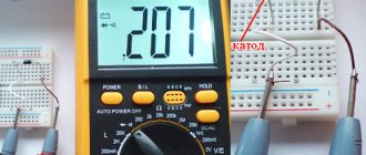
Schottky rectifiers can be tested in the same way as conventional semiconductors, since they have similar characteristics. You need to ring it in both directions with a multimeter - it should show itself in the same way as a regular diode: anode-cathode, and there should be no leaks. If it shows even a slight resistance - 2-10 kilo-ohms, this is already a reason for suspicion.
Checking a Schottky diode with a multimeter
A diode with a common anode or cathode can be tested like two ordinary semiconductors connected together. For example, if the anode is common, then it will be one leg out of three. We place one tester probe on the anode, the other legs are different diodes, and another probe is placed on them.
Can it be replaced with another type? In some cases, Schottky diodes are replaced with ordinary germanium diodes. For example, D305 at a current of 10 amperes gave a drop of only 0.3 volts, and at currents of 2–3 amperes they can generally be installed without radiators. But the main purpose of the Schottky installation is not a small drop, but a low capacity, so replacement will not always be possible.
As we see, electronics does not stand still, and further applications of high-speed devices will only increase, making it possible to develop new, more complex systems.
Schottky diodes, or more precisely Schottky barrier diodes, are semiconductor devices made on the basis of a metal-semiconductor contact, while conventional diodes use a semiconductor pn junction.
The Schottky diode owes its name and appearance in electronics to the German physicist and inventor Walter Schottky, who in 1938, while studying the newly discovered barrier effect, confirmed the previously put forward theory, according to which although the emission of electrons from a metal is prevented by a potential barrier, but as the applied external electric field, this barrier will decrease. Walter Schottky discovered this effect, which was then called the Schottky effect, in honor of the scientist.
Examining the contact between a metal and a semiconductor, one can see that if near the surface of the semiconductor there is a region depleted of major charge carriers, then in the region of contact of this semiconductor with the metal on the side of the semiconductor, a region of space charge of ionized acceptors and donors is formed, and a blocking contact is realized - the same Schottky barrier . Under what conditions does this barrier arise? Thermionic emission current from the surface of a solid body is determined by the Richardson equation:
Let us create conditions when, when a semiconductor, for example n-type, comes into contact with a metal, the thermodynamic work function of electrons from the metal would be greater than the thermodynamic work function of electrons from the semiconductor. Under such conditions, in accordance with the Richardson equation, the thermionic emission current from the surface of the semiconductor will be greater than the thermionic emission current from the metal surface:
At the initial moment of time, upon contact of the named materials, the current from the semiconductor to the metal will exceed the reverse current (from the metal to the semiconductor), as a result of which space charges will begin to accumulate in the near-surface regions of both the semiconductor and the metal - positive in the semiconductor and negative in the semiconductor. metal An electric field formed by these charges will arise in the contact area, and the energy zones will bend.
Under the influence of the field, the thermodynamic work function for the semiconductor will increase, and the increase will occur until the thermodynamic work functions and the corresponding thermionic emission currents in relation to the surface are equalized in the contact region.
Reverse recovery time
The most important difference between a n-p diode and a Schottky diode is the reverse recovery time (trr), when the diode switches from a conducting state to a non-conducting state. In a p−n diode, the reverse recovery time can range from a few microseconds to less than 100 ns for fast diodes, and it is mainly limited by the diffusion capacitance caused by minority carriers accumulated in the diffusion region during the conducting state.[3] Schottky diodes are significantly faster because they are unipolar devices and their speed is limited only by the junction capacitance. Switching time is ~ 100 for small-signal diodes and up to tens of nanoseconds for special high-power high-capacity diodes. When switching a p–n junction, a reverse recovery current also arises, which in power semiconductors increases EMI noise. Schottky diodes switch almost instantly with little capacitive load, which is not a concern.
This "instant" switching does not always happen. Particularly in higher voltage Schottky devices, the guard ring structure required to control the breakdown field geometry produces a parasitic pn diode with the usual recovery time attributes. As long as this protection ring diode is not forward biased, it only adds capacitance. However, if the Schottky junction is driven hard enough, the forward voltage will eventually drive both diodes forward and the actual trr will be greatly affected.
It is often said that the Schottky diode is a "primary operator" semiconductor device. This means that if the semiconductor body is n-type doped, only n-type carriers (mobile electrons) play a significant role in the normal operation of the device. Most carriers are quickly introduced into the conduction band of the metal contact on the other side of the diode to become free-moving electrons. Therefore, there is no slow random recombination of n- and p-type carriers, so this diode can stop conducting faster than a conventional p−n rectifier. diode. This property, in turn, allows the device footprint to be reduced, which also contributes to faster transition times. This is another reason why Schottky diodes are useful in pulsed mode. Power Converters: The diode's high speed means that the circuit can operate at frequencies ranging from 200 kHz to 2 MHz, allowing the use of small inductors and capacitors with greater efficiency than would be possible with other types of diodes. Small area Schottky diodes are the heart of RF detectors and mixers, often operating at frequencies up to 50 GHz.