Register Login
Publication date: October 31, 2013
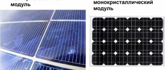
Currently, about 80-85% of solar cell production comes from crystalline modules. But according to experts in this field, the future still lies with thin-film technology. Its main advantage, which can provide it with a leading position, is its lower cost. Modules produced using thin-film technology are called flexible solar panels, due to the fact that their elasticity and low weight allow solar modules to be mounted on any surface and even sewn into clothing.
For the production of flexible modules, films made of polymer materials, amorphous silicon, aluminum, cadmium telluride and other semiconductors are used. Most often they are used as portable chargers, so-called folding solar panels, for laptops, video cameras, mobile phones and other electronics that do not require high power. To generate a significant amount of energy, a large area of modules will be required.
Review
Today, thin-film solar batteries, in addition to the classic installation on roofs, can be used instead of glazing. Such modules are distinguished by a variety of colors, which allows buildings to give a unique appearance.
Energy generated by thin-film batteries can be used for domestic needs.
The tempered glass covering the photocells has greater mechanical strength than regular glass and is safer. Therefore, the upper floors of houses in many countries, as well as loggias and balconies, are glazed with it.
In addition, it provides fairly good transparency, guaranteeing high efficiency even in diffuse light, i.e. They not only look aesthetically pleasing, but also save money.
For an opaque battery you will have to pay about 9 thousand rubles, for a partially transparent colored battery (20%) - 16 thousand.
But these days, thin-film solar cells are not as widespread as their crystalline brothers. The reasons lie in their large dimensions and low efficiency.
Nevertheless, experts believe that the future of solar energy lies with them.
They cite the following advantages of thin-film batteries:
- low cost;
- slight difference in efficiency;
- constant increase in the cost of crystalline analogues.
In addition, thin film technology is considered the most reliable. Already today, several types of thin-film batteries, also called “flexible”, have been developed, for the creation of which they use:
- amorphous silicon;
- cadmium telluride/sulfide;
- copper-indium and copper-helium diselenide.
Comments:
Megavolt
I read that they released solar batteries in the shape of a round cone, they produce 20% more than conventional batteries. Does anyone know about this technology?
Electrician
Megavolt, let's calculate))) The efficiency of film batteries (namely, they are rolled into a cone) = 10%. We add 20% of 10% to them and get as much as 12% with an increase in cost of at least three times! Breakthrough in savings!
Semyon
Electrician, I also watched this story. It immediately seemed suspicious to me that the entire scientific breakthrough consisted of giving batteries some kind of shape. As if no one had guessed before that the sun was out of place... As always - conspiracy theories and collusion.
Leave a comment Cancel reply
Related Posts
Photo manual: DIY solar battery step by step
Do solar panels for a private home pay off?
Types of solar-powered garden lamps and lanterns, how and where to use them.
The principle of operation of solar panels.
Main advantages
This type of thin-film solar panels has many differences from their crystalline counterparts:
- small thickness not exceeding 1 micron;
- excellent flexibility, allowing the panel to be mounted on all kinds of curved surfaces, including cylindrical ones;
- preservation of parameters in diffused light, which will increase the total power generation, in comparison with poly- and monocrystalline panels, by 10, and in some cases by 15 percent;
- low cost of the production process, therefore, low cost of the finished product;
- highly efficient operation in power systems with a power of more than 10 kW and in high temperature conditions;
- significant indicators of optical absorption of the solar spectrum, exceeding the crystalline spectrum by more than 20 times;
- stability of output power for a long time - reliability;
- environmentally friendly, since they have a low proportion of silicon used - 1/000 of that used in crystalline analogues;
- short payback period due to high energy output;
- light weight for easy installation;
- impact resistance. During installation, falls are common, but the film remains operational.
Efficiency of thin film amorphous silicon panels
Initially, if we compare the power output of thin film panels and crystalline silicon panels, the figure does not favor thin films: 18-22% versus about 7-8%. This low efficiency is partly due to the Stabler-Wronski effect (photoinduced degradation), which occurs in the first hours when the panels are exposed to sunlight. This phenomenon causes the energy output of the amorphous silicon panel to decrease from 10 percent to about 7 percent.
However, with the development of technology in recent years, these indicators are rapidly improving. Today, scientists and engineers working to improve the panels have gradually brought the efficiency of amorphous panels to 12.5% in the laboratory. The efficiency of amorphous silicon solar cells, which are produced in large volumes, ranges from 6% to 9%.
Currently, there are three generations of thin-film panels based on amorphous silicon.
1st generation. This includes the ancestor of the technology - the single-junction solar battery. It is characterized by a short service life (up to 10 years) and a low level of productivity (about 5%).
2nd generation. The same single-junction solar battery with increased efficiency (up to 8%).
3rd generation. The most highly efficient thin-film amorphous panels available today with a service life of over 10 years and a performance level of 12-12.5%.
Most often, thin-film panels are used for solar systems operating on an industrial scale with dependent (slave, grid-tie) inverters and supplying electricity to the general network, since amorphous modules show the greatest efficiency when used in powerful systems (from 10 kW).
Device
Triplexes made of tempered glass, in which thin-film solar panels are placed, are reliable protection for the latter. The photographic film is placed under high-strength glass, which is highly transparent and at the same time transparent. The same solution is used in the automotive industry, the production of LED triplexes, and architecture, where it has proven itself to be the best.
We recommend:
- Solar panels work at night and in cloudy weather
- Monocrystalline solar panels: comparison with analogues, advantages, price - TOP-6
- Goal Zero Nomad 14 Plus: solar panel review, appearance, device, advantages and price
About technology
To make a thin-film solar structure, semiconductor compounds are sputtered onto a flexible substrate (usually a polymer).
At first, they used exclusively amorphous silicon for this. But, I was not satisfied with the low efficiency of photocells - about 4-5%.
After the advent of selenide and telluride - innovative materials, it was possible to achieve a higher efficiency rate - up to 12%.
Disadvantages of thin film solar cell
- High cost when compared with classic batteries. If the cost is the same, then batteries of this type produce three times less power, which cannot be called optimal.
- Low efficiency. Here you can even give a simple example: if you install such a film on a window, it is unlikely to be able to charge your phone. The output efficiency is only 4%, which is three times less than usual.
- It gets very hot, at a very hot temperature 30-40%, conventional ones show a result of only 12%.
Vacuum method
The method involves the use of vacuum chambers or electron guns for deposition of diselends from vapor.
In principle, any approach can be used, for example, ion sputtering, but all methods have their own difficulties, such as the formation of a film both on the substrate and on the inner surface of the chamber. Another difficulty is associated with the supply of indium, which is actively used for the manufacture of flat panel monitors.
For such devices, the efficiency can exceed 20%.
Although panels of this type are actively developing, their demand is small and does not exceed 2%.
Films made using cadmium telluride have gained great popularity. Their efficiency is 16% (versus 18%). Amorphous silicon batteries are very popular. Their efficiency was increased to 10%.
HiSoUR Cultural history
A thin film solar cell is a second generation solar cell that is created by depositing one or more thin layers or thin film (TF) of photovoltaic material onto a substrate such as glass, plastic or metal. Thin-film solar cells are commercially used in several technologies, including cadmium telluride (CdTe), copper indium gallium dieselide (CIGS), and amorphous thin-film silicon (a-Si, TF-Si).
Film thicknesses range from a few nanometers (nm) to tens of micrometers (µm), much thinner than competing thin film technology, the traditional first-generation crystalline silicon solar cell (c-Si), which uses wafers up to 200 µm. This allows thin-film cells to be flexible and weigh less. It is used in the construction of integrated photovoltaic cells and as a translucent, photovoltaic glazing material that can be laminated onto windows. Other commercial applications use rigid thin-film solar panels (sandwiched between two glasses) in some of the world's largest photovoltaic power plants.
Thin film technology has always been cheaper but less efficient than traditional c-Si technology. However, it has improved significantly over the years. Laboratory cell efficiency for CdTe and CIGS now exceeds 21 percent, surpassing multicrystalline silicon, the dominant material currently used in most solar photovoltaic systems. 23.24. Accelerated life testing of thin film modules in laboratory conditions showed slightly faster degradation compared to conventional PV, while a 20-year life period is typically expected. Despite these improvements, thin film market share has not reached more than 20 percent in the last two decades and has been declining in recent years, to about 9 percent of global photovoltaic installations in 2013. 18.19
Other thin film technologies that are still in the early stages of ongoing research or with limited commercial availability are often classified as new or third generation photovoltaic cells and include organic, dye-sensitized and polymer solar cells, as well as quantum dots, copper zinc tin sulfide, nanocrystal , micromorph and perovskite solar cells.
Types Many of the photovoltaic materials are made with different deposition methods on different substrates. Thin film solar cells are usually classified according to the photovoltaic material used:
Amorphous silicon (a-Si) and other thin film silicon (TF-Si) Cadmium telluride (CdTe) Copper indium gallium and selenium (CIS or SIGS) Dye sensitized solar cells (DSC) and other organic solar cells.
history Thin film cells have been well known since the late 1970s, when solar calculators with a small strip of amorphous silicon appeared on the market.
It is now available in very large modules used in complex integrated buildings and vehicle charging systems.
Although thin film technology is expected to achieve significant market success and surpass the dominant traditional crystalline silicon (c-Si) technology in the long term, market share has been declining for several years. While in 2010, when there was a shortage of conventional PV modules, thin film made up 15 percent of the total market, it fell to 8 percent in 2014 and is expected to stabilize at 7 percent from 2015, expected to amorphous silicon will lose half its market share by the end of the decade.
materials Thin film technologies reduce the amount of active material in the cell. Most of the active substances are sandwiched between two glasses. Because silicon solar panels use only a single pane of glass, thin-film panels are approximately twice as heavy as crystalline silicon panels, although they have a lower environmental impact (determined from life cycle analysis). Most film panels have 2-3 percentage points lower conversion efficiency than crystalline silicon. Cadmium telduride (CdTe), copper gallium selenide (CIGS), and amorphous silicon (a-Si) are three thin film technologies often used for outdoor applications.
Cadmium Telluride Cadmium telluride (CdTe) is the predominant thin film technology. With about 5 percent of global PV production, it accounts for more than half of the thin film market. Laboratory cell efficiency has also increased significantly in recent years and is on par with thin film CIGS and close to the efficiency of multicrystalline silicon as of 2013. 24-25 In addition, CdTe has the lowest energy payback time of all mass-PV manufacturing technologies and can be short, like eight months, in favorable places. 31. A well-known manufacturer is the American company First Solar, based in Tempe, Arizona, which produces CdTe panels with an efficiency of about 14 percent at a reported cost of $0.59 per watt.
Although cadmium toxicity may not be that big of a problem and environmental concerns have been completely resolved by recycling CdTe modules at the end of their life, there are still uncertainties and public opinion is skeptical about this technology. The use of rare materials may also be a limiting factor in the industrial scalability of CdTe thin film technology. The rarity of tellurium, of which telluride is the anionic form, is comparable to that of platinum in the earth's crust and significantly influences the cost of the module.
Copper indium gallium selenide The copper indium gallium selenide solar cell or CIGS cell uses a copper indium gallium selenide (CIGS) absorber, while gallium variants of the semiconductor material are abbreviated CIS. It is one of three major thin-film technologies, the other two being cadmium telluride and amorphous silicon, with laboratory efficiency above 20 percent and a 2 percent share of the overall PV market in 2013. A well-known manufacturer of cylindrical CIGS panels was now bankrupted by Solyndra in Fremont, California. Traditional manufacturing methods include vacuum processes including co-evaporation and atomization. In 2008, IBM and Tokyo Ohka Kogyo Co., Ltd. (TOK) announced that they have developed a new, non-vacuum, solution-based process for the production of CIGS cells and are targeting efficiency gains of 15% or more.
Hyperspectral imaging was used to characterize these cells. Researchers from IRDEP (Institute for Photovoltaic Energy Research and Development) in conjunction with Photon etc. were able to determine the quasi-Fermi level splitting with photoluminescence imaging, while the electroluminescence data was used to obtain the external quantum efficiency (EQE). Additionally, in In the light beam-based mapping (LBIC) experiment, the EQE of a CIGS microcrystalline solar cell could be determined at any point in the field of view.
As of September 2014, the current conversion efficiency rate for the CIGS laboratory cell is 21.7%.
Silicon Three main silicon-based modules dominate:
amorphous silicon cells amorphous/microcrystalline tandem cells (micromorph) thin film polycrystalline silicon on glass.
Amorphous Silicon Amorphous silicon (a-Si) is a non-crystalline, allotropic form of silicon and the most well-developed thin film technology. Thin film silicon is an alternative to traditional wafer-like (or bulk) crystalline silicon. Although CdTe chalcogenide cells and CIS thin films have been developed in the laboratory with great success, silicon thin film cells continue to attract industry interest. Silicon-based devices have fewer problems than their CdTe and CIS competitors, such as toxicity and moisture issues with CdTe cells and low LPG manufacturing yields due to material complexity. Additionally, because of the political resistance to using non-green materials in solar energy production, there is no stigma in using standard silicon.
This type of thin film cell is primarily made using a technology called plasma chemical vapor deposition. It uses a gas mixture of silane (SiH4) and hydrogen to deposit a very thin layer of only 1 micrometer (µm) of silicon on a substrate such as glass, plastic or metal that is already coated with a layer of transparent conductive oxide. Other methods used to deposit amorphous silicon onto a substrate include sputtering and chemical vapor deposition methods.
a-Si is attractive as a solar cell material because it is an abundant, non-toxic material. It requires low processing temperature and enables scalable production on a flexible, low-cost substrate with a small amount of silicon material. Because of its 1.7 eV bandgap, amorphous silicon also absorbs a very wide range of light spectrum, which includes infrared and even some ultraviolet, and works great in low light. This allows the cell to generate energy in the early morning or late afternoon, as well as on cloudy and rainy days, unlike crystalline silicon cells, which are significantly less efficient when exposed to diffuse and indirect daylight.
However, during the first six months of operation, the efficiency of the a-Si cell decreases significantly by 10-30%. This is called the Staebler-Wronski effect (SWE) - a typical loss of electrical power due to changes in photoconductivity and dark conductivity caused by long-term exposure to sunlight. Although this degradation is completely reversible when annealed at or above 150 °C, conventional c-Si solar cells do not exhibit this effect in the first place.
Its main electronic structure is a contact junction. The amorphous structure of a-Si implies high intrinsic disorder and dangling bonds, making it a poor conductor of charge carriers. These dangling bonds act as recombination centers that significantly reduce the lifespan of the host. Typically a pin structure is used as opposed to a clamp structure. This is because the electron mobility in a-Si:H is about 1 or 2 orders of magnitude greater than the hole mobility, and hence the collection rate of electrons moving from an np-type contact is better than holes moving from a p contact -to-n. Therefore, the p-type layer must be located at the top, where the light intensity is stronger, so that most of the charge carriers crossing the junction are electrons.
Tandem cell using a-Si/μc-Si A layer of amorphous silicon can be combined with layers of other allotropic forms of silicon to create a multi-component solar cell. When only two layers (two pn junctions) are combined, it is called a tandem cell. By stacking these layers on top of another, a wider spectrum of light is absorbed, improving the overall efficiency of the cell.
In micromorphic silicon, a layer of microcrystalline silicon (μc-Si) is combined with amorphous silicon to create a tandem cell. The top a-Si layer absorbs visible light, leaving the infrared portion to the bottom μc-Si layer. The micromorphic stacked cell concept was first introduced and patented at the Institute of Microtechnology (IMT) at the University of Neuchâtel in Switzerland and licensed to TEL Solar. A new world-class optical module based on the micro-moroc concept with a module efficiency of 12.24% was independently certified in July 2014.
Since all layers are made of silicon, they can be manufactured using PECVD. The gap between a-Si is 1.7 eV, and c-Si is 1.1 eV. The C-Si layer can absorb red and infrared light. The best efficiency can be achieved by switching between a-Si and c-Si. Since nanocrystalline silicon (nc-Si) has approximately the same bandgap as c-Si, nc-Si can replace c-Si.
Tandem cell using a-Si/pc-Si Amorphous silicon can also be combined with protocrystalline silicon (pc-Si) into a tandem cell. Protocrystalline silicon with a low volume fraction of nanocrystalline silicon is optimal for high open-loop voltage. These types of silicon present dangling and twisted bonds, resulting in deep defects (band gap energy levels) as well as valence and conduction band deformation (ribbon tails).
Polycrystalline silicon on glass A new attempt to fuse the benefits of bulk silicon with thin-film device materials is thin film polycrystalline silicon on glass. These modules are fabricated by depositing anti-reflection coating and doped silicon onto textured glass substrates using plasma chemical vapor deposition (PECVD). The texture in the glass increases cell efficiency by approximately 3% by reducing the amount of incident light reflected from the solar cell and trapping light within the solar cell. The silicone film crystallizes at the annealing stage, temperature 400-600 Celsius, resulting in the formation of polycrystalline silicon.
These new devices show energy conversion efficiencies of 8% and high production yields of >90%. Crystalline silicon on glass (CSG), where polycrystalline silicon is 1-2 micrometers, is noted for its stability and durability; The use of thin film technologies also contributes to cost savings for bulk photovoltaic cells. These modules do not require a transparent conductive oxide layer. This simplifies the production process by half; Not only can this step be skipped, but the absence of this layer makes the process of constructing the pin diagram much easier. Both of these simplifications further reduce production costs. Despite numerous advantages over alternative designs, estimates of manufacturing costs per unit area indicate that these devices are comparable in cost to single-component amorphous thin-film cells.
Gallium Arsenide The semiconductor material gallium arsenide (GaAs) is also used for single-crystal thin-film solar cells. Although GaAs cells are very expensive, they hold the world record for high efficiency single-component solar cell at 28.8%. GaAs is more commonly used in multi-cell solar cells for solar panels on spacecraft as the industry promotes efficiency gains through the use of space-based solar power (InGaP/(In)GaAs/Ge). They are also used in concentrator photovoltaics, a newer technology most suitable for locations that receive a lot of sunlight, using lenses to focus sunlight onto a much smaller, therefore less expensive, GaAs solar concentrator cell.
Emerging Photovoltaics The National Renewable Energy Laboratory (NREL) classifies a number of thin-film technologies as emerging photovoltaics—most of which are still not in commercial use and are in the research or development stages. Many use organic materials, often organometallic compounds, as well as inorganic substances. Although their efficiency was low and the stability of the absorber material was often too short for commercial applications, much research is being put into these technologies as they promise to achieve the goal of producing low-cost, high-efficiency solar cells.
New photovoltaics, often called third generation photovoltaic cells, include:
Copper-zinc tin sulfide solar cell (CZTS) and derivatives CZTSe and CZTSSe Dye sensitized solar cell, also known as "Gretzel cell", Organic solar cells Perovskite solar cell Polymer solar cell Quantum dot solar cell
In particular, advances in perovskite cell research have received enormous public attention as their research efficiency has recently skyrocketed above 20 percent. They also offer a wide range of low-cost apps. Additionally, another new technology, concentrator photovoltaics (CPV), uses high-efficiency multi-cell solar cells combined with optical lenses and a tracking system.
Efficiency Incremental improvements in efficiency began with the invention of the currently first silicon solar cell in 1954. By 2010, these steady improvements resulted in modules capable of converting 12 to 18 percent of solar radiation into electricity. Efficiency improvements have continued to accelerate since 2010, as shown in the accompanying chart.
Cells made from newer materials tend to be less efficient than bulk silicon but are less expensive to produce. Their quantum efficiency is also lower due to the reduced number of charge carriers collected per incident photon.
The performance and potential of thin film materials is high, achieving cellular efficiency of 12-20%; efficiency of the prototype module is 7-13%; and production modules in the 9% range. The best efficiency thin film cell prototype produces 20.4% (First Solar), which compares to Panasonic's best standard solar cell prototype of 25.6%.
NREL once [when?] predicted that costs would fall below $100/m2 in production volume and could later fall below $50/m2.
A new thin film solar cell efficiency record of 22.3% has been achieved thanks to the solar frontier of the world's largest solar energy supplier. In joint research with the New Energy and Industrial Development Organization (NEDO) of Japan, the solar frontier achieved 22.3% conversion efficiency on a 0.5 cm2 cell using its CIS technology. This is an increase of 0.6 percentage points over the industry's previous thin film growth of 21.7%.
absorption To increase the amount of light entering a cell, several techniques have been used to reduce the amount that escapes without absorption. The most obvious method is to minimize the coverage of the top contact surface of the cell, reducing the area that blocks light from entering the cell.
Weakly absorbed long-wavelength light can be obliquely coupled to the silicon and cross the film several times to enhance absorption.
Several methods have been developed to increase absorption by decreasing the number of photons reflected from the cell surface. The additional anti-reflective coating can cause damaging interference within the cell by modulating the refractive index of the surface coating. The disruptive interference eliminates the reflective wave, causing all incident light to enter the cell.
Surface texturing is another option to increase absorption, but increases costs. By applying the texture to the surface of the active material, the reflected light can be refracted when striking the surface, which reduces the reflectance. For example, black silicon texture by reactive ion etching (RIE) is an effective and cost-effective approach to enhance the absorption of thin-film silicon solar cells. A textured rear reflector may block light from passing through the back of the cell.
In addition to surface texturing, plasma light trapping scheme has attracted much attention to photocurrent enhancement in thin film solar cells. This method uses the collective vibrations of excited free electrons in noble metal nanoparticles, which are influenced by the particle shape, size and dielectric properties of the surrounding medium.
In addition to minimizing reflective losses, the solar cell material can be optimized to have a higher probability of absorbing a photon that reaches it. Thermal treatment methods can significantly improve the quality of silicon cell crystals and thereby increase efficiency. Layered thin film cells can also be made to create a multi-beam solar cell. The band gap between the layers can be designed to best absorb a different range of wavelengths, so that together they can absorb a larger spectrum of light.
Further advances in geometric considerations may favor the dimensionality of nanomaterials. Large parallel arrays of nanowires allow absorption lengths to extend along the length of the wire while maintaining short minority carrier diffusion distances along the radial direction. Adding nanoparticles between the nanowires enables conduction. The natural geometry of these arrays creates a textured surface that captures more light.
Production, Cost and Market Due to advances in conventional crystalline silicon (c-Si) technology in recent years and falling costs of polysilicon raw materials following a period of severe global shortages, pressure is placed on manufacturers of commercial thin-film technologies, including amorphous thin-silicon (a-Si) , cadmium telluride (CdTe) and copper gallium diselenide (CIGS), leading to the bankruptcy of several companies. Since 2013, thin film producers continue to face price competition from Chinese silicon refineries and traditional c-Si solar panel manufacturers. Some companies, along with their patents, were sold to Chinese firms at cost.
Market Share In 2013, thin film technologies accounted for about 9 percent of global deployment, while crystalline silicon (mono-Si and multi-Si) accounted for 91 percent. With 5% of the overall market, CdTe owns more than half of the thin-film market, leaving 2 percent each for CIGS and amorphous silicon. 18-19
CIGS Technology Several well-known manufacturers have succumbed to the pressure caused by the advances in conventional c-Si technology in recent years. Solyndra ceased all operations and filed for Chapter 11 bankruptcy in 2011, and Nanosolar, also a CIGS manufacturer, closed its doors in 2013. Although both companies produced CIGS solar cells, it was stated that the failure was not caused by the technology, but rather by the companies themselves, exploiting architectural flaws such as Solyndra's cylindrical substrates. In 2014, Korean company LG Electronics stopped research into CIGS reorganization of its solar business, and Samsung SDI decided to cease production of CIGS, while Chinese PV manufacturer Hanergy is expected to increase production capacity of its 15.5% effective 650 mm × 1650 mm CIGS modules. One of the largest manufacturers of CI(G)S photovoltaics is the Japanese company Solar Frontier, with gigawatt-scale production capacity. (Also see List of CIGS companies).
CdTe Technology First Solar, a leading CdTe producer, is building some of the world's largest solar power plants, such as the Desert Sunlight solar farm and the Topaz solar farm, both in the California desert with a capacity of 550 MW each, and the 102 MW Nyngan Solar plant in Australia , the largest PV power plant in the Southern Hemisphere, commissioned in 2015. In 2011, GE announced plans to spend $600 million on a new CdTe solar cell plant and enter that market, and in 2013, First Solar bought GE's thin-film CdTe intellectual property portfolio and formed a business partnership. In 2012, Abound Solar, a manufacturer of cadmium telluride modules, went bankrupt.
a-Si Technology In 2012, ECD solar, one of the world's leading producers of amorphous silicon (a-Si), filed for bankruptcy in Michigan, USA. Swiss OC Oerlikon divested its solar division that produced a-Si/μc-Si tandem cells to Tokyo Electron Limited. In 2014, the Japanese electronics and semiconductor company announced the closure of its micromorph technology development program. "Micromorph" was the commercial name for a solar tandem cell using a layer of microcrystalline silicon over an amorphous layer (a-Si/μ-Si). Other companies that have exited the amorphous silicon thin film market include DuPont, BP, Flexcell, Inventux, Pramac, Schuco, Sencera, EPV Solar, NovaSolar (formerly OptiSolar) and Suntech Power, which stopped producing Si-Si modules in 2010 to focus on traditional silicon solar panels. In 2013, Suntech filed for bankruptcy in China. In August 2013, spot prices for thin-film a-Si and a-Si/μ-Si fell to €0.36 and €0.46, respectively (about $0.50 and $0.60) per watt.
Share link:
- Click to share on Twitter (Opens in new window)
- Click here to share content on Facebook. (Opens in a new window)
- Click to share on Pinterest (Opens in new window)
- Click to share posts on Tumblr (Opens in new window)
- Click to share on LinkedIn (Opens in new window)
- Click to share on WhatsApp (Opens in new window)
- Click to share on Skype (Opens in new window)
- Click to share on Telegram (Opens in new window)
- Click to share on Reddit (Opens in new window)
- Click to share posts on Pocket (Opens in new window)
Related
Share: Twitter Facebook Google+
Suspension method
In the production of thin-film solar cells, leading specialists use several methods for applying diselenides. The most common is the use of suspended metal oxides.
By changing the concentration and viscosity of the suspension, so-called “ink” is obtained, which is adjusted for a specific technology (from screen printing to jet deposition).
Various materials can also serve as a substrate - metallized foil, glass, even plastic. The efficiency of using the material is very high - 90%, and production is many times cheaper than vacuuming.
The advantage of the method is a uniform and homogeneous spray layer, but the disadvantage is low, compared to vacuum, efficiency - 16% (versus 18%).
Multijunction Solar Cells
Most solar cells currently produced have a single pn junction. That is, free electrons in such an element create only those photons that have an energy greater than or equal to the band gap. To overcome this limitation, scientists have developed a new type of solar cells called cascade cells. They have a multilayer structure consisting of solar cells with different band gaps.
The most promising flexible solar cells made using cascaded cells have 3 pn junctions. The top layer is formed from an alloy based on a-Si:H, for the second layer an a-SiGe:H alloy containing 10-15% germanium is used, for the third layer the percentage of germanium in the alloy is increased to 40-50%. With each subsequent layer, the band gap decreases, so each subsequent layer absorbs those photons that passed through the previous one. The table below shows the efficiency values of cascade solar cells. It is worth noting that such high efficiency indicators make it possible to reduce the cost of generated solar energy by almost 2 times in comparison with solar batteries based on crystalline silicon.
| Theoretical efficiency value | Expected efficiency value | Realized efficiency value | |
| 1 pn junction | 30 | 27 | 25,1 |
| 2 pn junctions | 36 | 33 | 30,3 |
| 3 pn junctions | 42 | 38 | 31,0 |
| 4 pn junctions | 47 | 42 | — |
| 5 pn junctions | 49 | 44 | — |