In the article “TL494, what kind of “beast” is this?”, we looked at the TL494 PWM controller. In this article we will look at no less, and probably even more common, PWM controllers of the 184x, 284x, 384x series. All these PWM controllers are designed to build switching power supplies for REA, with current and voltage regulation, to control the key stage on an n-channel MOS transistor. In principle, these are the same controllers, differing only in the operating temperature range in which these controllers operate reliably.
The 184x series controllers have the largest operating temperature range, which reaches -55…+125°C. The 284x series controllers have an operating temperature range of -40...+85°C, which is also not bad, and naturally they will all be more expensive than the 384x series controllers, since the smallest operating temperature range is precisely that of the 384x series controllers, which is 0...+70°C, then These controllers are designed primarily for installation in equipment operating indoors. Domestic analogues for these controllers are as follows;
For x842 controllers - KR1033EU10, K1033EU15A, 1114EU7/IM.
For x843 controllers - K1033EU15B, 1114EU8/IM.
For x844 controllers - KR1033EU11, K1033EU16A, 1114EU9/IM.
For x843 controllers - K1033EU16B, 1114EU10/IM.
The operating temperature range of domestic analogues is as follows; For controllers of the 1033EUxx series - ranges from -10 to +70°C. In some “datasheets” the lower operating threshold of these controllers is indicated from 0°C. That is, this series is a complete analogue of the 384x series controllers. For controllers of the 1114EUxx series, the operating temperature range is from -60 to +125 °C
By tradition, let's see what it has inside.
Introduction
The mains power supply is one of the most critical components in the structure of electronic equipment.
The most important parameters of a network converter are: operating range of input voltage, power consumption in standby mode, overall dimensions, reliability, electromagnetic compatibility and cost. The vast majority of modern mains-powered equipment uses switching power supplies. The network switching power supply provides galvanic isolation of the output circuits from the mains voltage. Isolation is ensured by using a pulse transformer in the power circuit and an optocoupler in the feedback circuit. The key element of a switching network power supply is a PWM controller chip. The main function of a PWM controller is to control the power transistor (transistors) located in the primary circuit of the pulse transformer and maintain the output voltage at a given level using a feedback signal. The structure of modern PWM controllers also provides additional functions that increase the efficiency and reliability of the power supply:
- limiting the current and duty cycle of pulses in the control circuit of power transistors;
- smooth start of the converter after power supply (Soft Start);
- built-in dynamic power supply from high voltage input voltage;
- control of the input voltage level with the elimination of “dips” and “overshoots”;
- short circuit protection in the power transformer circuit and output circuits of the output rectifier;
- temperature protection of the controller, as well as the key element;
- blocking the operation of the converter at low and high input voltage;
- optimization of control for standby mode and mode with reduced current in the load (skipping cycles or switching to a lower conversion frequency);
- optimization of EMR levels.
The PWM controllers discussed in the article do not have a built-in power transistor that controls the current in the primary circuit of the power transformer.
Compound.
It contains:
— 5V reference voltage source with external pin 8; — power supply voltage undervoltage protection circuit (UVLO). — sawtooth voltage generator (generator); — current comparator, used mainly for the current limit signal; — error amplifier, used mainly for voltage; — control circuit for the operation of the output stage;
The UCx844 and UCx845 chips have a built-in counting trigger (indicated by a dotted line), which serves to obtain a maximum duty cycle (PWM duty cycle) of 50%. Therefore, for the master oscillators of these microcircuits, you need to set the switching frequency twice as high as necessary. The UCx842 and UCx843 microcircuit generators are set to the required switching frequency. The maximum operating frequency of the master oscillators of the UCx842/3/4/5 family of controllers can reach 500 kHz. How else do these microcircuits differ from each other? These are different supply voltages for these microcircuits. See the table below;
| ON VOLTAGE – 16 V, OFF – 10 V | ON VOLTAGE – 8.4 V, OFF – 7.6 V | OPERATING TEMPERATURE RANGE | FULL RATIO DUTY CYCLE |
| UC1842 | UC1843 | -55°С… +125°С | up to 100% |
| UC2842 | UC2843 | -40°С… +85°С | |
| UC3842 | UC3843 | 0°С… +70°С | |
| UC1844 | UC1845 | -55°С… +125°С | up to 50% |
| UC2844 | UC2845 | -40°С… +85°С | |
| UC3844 | UC3845 | 0°С… +70°С | |
Also, microcircuits with the suffix “A”, for example UC3842A, have half the trigger current - 0.5 mA. Microcircuits without the “A” suffix have a starting current of about 1.0 mA. Yes, I completely forgot about the microcircuit housings. Here we are mainly considering microcircuits in an eight-pin DIP-8 package (there may be a suffix “N”, or a ceramic CERDIP-8 package (suffix “J”), or a SOIC-8 package (suffix “D8”). The pinouts of the eight-pin microcircuits are completely the same.The microcircuits can also be produced in a 14-pin “SOIC-14” package, with the suffix “D”, and can also be in a “PLCC-20” package (suffix “Q”). The pinouts of the microcircuits in these cases are different. Domestic microcircuits of the 1114 series are made in the H02.8-2B package. This is a ten-pin metal-ceramic package (below in the figure) with five pins on each side, the middle pins of which are simply a technological jumper and not are taken into account, that is, the same eight conclusions are obtained.
Now you can determine by the marking what kind of microcircuit it is, for example UC3843AD; - this is a PWM controller with a reduced startup current (500 μA), with switching on when the supply voltage reaches 8.4 volts and turning off when the supply voltage threshold reaches 7.6 volts, with a duty cycle of up to 100% and is made in the “SOIC” package -14".
Basic parameters of the power stage control mode
Depending on the requirements of a specific application, the controller can use different circuits of the power switch control output stage, the type of feedback circuit control (current or voltage), as well as different frequency conversion modes. The type of output stage of the PWM controller also determines the topology of the converter.
Types of network converter topologies:
- flyback;
- straight forward;
- push-pull;
- half-bridge;
- pavement;
- quasi-resonant.
Table 1 shows the characteristics of the basic circuit topologies used in the construction of switching network power supplies.
Flyback converter
The basic circuit used in many low-power switching power supplies is a flyback converter (Fig. 1). This circuit converts one DC voltage to another by adjusting the output voltage through pulse width modulation (PWM) or pulse frequency modulation (PFM). Pulse width modulation is a control method based on changing the ratio of the duration of the switch on to the off state at a constant frequency. In a flyback converter, the duration of the switch's on state is longer than the duration of the off state so that more energy is stored in the transformer and transferred to the load.
Rice. 1. Typical flyback converter circuit
Forward converter
Another popular switching power supply configuration is known as a forward converter circuit and is shown in Fig. 2. Although this circuit is very similar to a flyback circuit, there are some fundamental differences. A forward converter stores energy not in a transformer, but in an output inductor (inductor). The dots marking the beginning of the windings on the transformer show that when the switching transistor is turned on, voltage appears in the secondary winding and current flows through the diode VD1 into the inductor. This circuit has a longer switch on time relative to the switch off state, a higher average voltage in the secondary winding and a higher output load current.
Rice. 2. Forward mains voltage converter
Push-pull forward converter
In Fig. Figure 3 shows a push-pull converter, which is a type of forward converter, except that both switches are included in the primary winding circuit of the transformer.
Rice. 3. Scheme of a push-pull forward converter
The range of ON Semi PWM controllers includes microcircuits with different output stage topologies, control types, frequency control modes, as well as additional built-in functions.
Table 2 presents the main parameters of ON Semi PWM controllers currently produced. Table 2. Main parameters of ON Semi PWM controllers for network switching power supplies
| Type | Topology | Regulatory mode | Frequency, kHz | Stand-by mode | Input undervoltage protection UVLO, V | Output short circuit protection | Blocking | Soft Start Mode |
| NCL30000 | Flyback | By current | Up to 300 | — | — | — | — | — |
| NCL30001 | Flyback | By current | Up to 150 | — | — | — | — | — |
| NCP1237 | Flyback | By current | 65 | — | — | + | + | + |
| NCP1238 | Flyback | By current | 65 | — | — | + | + | + |
| NCP1288 | Flyback | By current | 65 | — | 10 | + | + | + |
| NCP1379 | Flyback | By current | Varies | + | 9 | + | + | + |
| NCP1380 | Flyback | By current | Varies | + | 9 | + | + | + |
| NCP1252 | Forward | By current | Up to 500 | + | 9-10 | + | + | + |
| CS51221 | Forward | By voltage | Up to 1000 | — | + | — | + | + |
| CS5124 | Flyback | By current | 400 | — | + | — | — | + |
| MC33025 | Push-Pull | By current or voltage | 1000 | — | + | + | — | + |
| MC33060 | Flyback | By voltage | 200 | — | + | — | — | + |
| MC33067 | Flyback | By voltage | 1000 | — | + | + | — | + |
| MC33364 | Flyback | By current | Varies | + | + | — | — | — |
| MC34060 | Multimode | By voltage | 200 | — | + | — | — | — |
| MC34067 | Resonant | By voltage | — | — | + | + | — | — |
| MC44603 | Flyback | By current or voltage | Up to 250 | + | 9 | + | + | + |
| NCP1200 | Flyback | By current | 100 | + | — | + | — | — |
| NCP1203 | Flyback | By current | 100 | + | + | + | — | — |
| NCP1207 | Flyback | By current | Up to 1000 | + | + | + | + | + |
| NCP1216 | Flyback | By current | 100 | + | — | + | — | + |
| NCP1217 | Flyback | By current | 100 | + | + | + | + | + |
| NCP1219 | Flyback | By current | 100 | + | 9,4 | + | + | + |
| NCP1230 | Flyback | By current | 100 | + | + | + | + | + |
| NCP1252 | Flyback/Forward | By current | Up to 500 | + | 9-10 | + | + | + |
| NCP1271 | Flyback | By current | 100 | + | + | + | + | + |
| NCP1294 | Flyback | — | Up to 1000 | + | + | + | + | — |
| NCP1308 | Flyback | By current | Varies | + | + | + | + | + |
| NCP1337 | Flyback | By current | Varies | + | + | + | + | + |
| NCP1338 | Flyback | By current | Varies | + | + | + | + | + |
| NCP1351 | Flyback | By current | Varies | — | — | + | + | — |
| NCP1377 | Flyback | By current | Varies | + | + | — | + | + |
| NCP1379 | Flyback | By current | Varies | + | 9 | + | + | + |
| NCP1380 | Flyback | By current | Varies | + | 9 | + | + | + |
| NCP1381 | Flyback | By current | Varies | + | + | + | + | + |
| NCP1382 | Flyback | By current | Varies | + | + | + | + | + |
| NCP1392 | Half-Bridge | By current | 250 | — | 9 | — | — | + |
| NCP1393 | Half-Bridge | By current | 250 | — | 9 | — | — | + |
| NCP1395 | Push-Pull | By voltage | 1000 | + | + | + | + | + |
| NCP1396 | Push-Pull | By voltage | Up to 500 | + | + | + | + | + |
| NCP1397 A/B | Half-Bridge | By voltage | 50-500 | — | 9,5/10,5 | + | + | + |
| NCP1562 | Flyback | By voltage | Up to 500 | — | + | + | + | + |
| NCV3843, UC3843 | Flyback | By current | 52 | — | + | + | — | + |
| UC2842/43/44 | Flyback | By current | 52 | — | + | + | — | — |
| UC2843/44/45 | Flyback | By current | 52 | — | + | + | — | — |
| UC3842 /44/45 | Flyback | By current | 52 | — | + | + | — | — |
| UC3845 | Push-Pull | By current | 52 | — | + | + | — | + |
It should be noted that the structure of the latest PWM controller chips is very similar. The main differences are determined by the type of topology, control mode (current/voltage), frequency control mode (constant or variable frequency), as well as the operating logic when critical situations are detected. The structure of the PWM controller contains logic that defines the state machine. The transition machine circuit is implemented using comparators, flip-flops, timers and logic elements. The main states of the controller: initial start-up of the frequency generator, entering the operating mode, adaptive monitoring of the load current and selection of the optimal mode, detection of critical situations, transition to emergency mode, auto-recovery after failures.
Output control voltage (OUT)
The number of pins of a microcircuit is determined by its design and operating principle. It’s not always possible to immediately understand complex terms, but let’s try to highlight the essence. There are microcircuits on 2 pins that control push-pull (double-arm) cascades (examples: bridge, half-bridge, 2-stroke inverse converter). There are also analogues of PWM controllers for controlling single-ended (single-arm) cascades (examples: forward/reverse, boost/buck, inverting).
In addition, the output stage can be single- or two-cycle in structure. Push-pull is mainly used to drive a voltage dependent FET. To quickly close, it is necessary to achieve rapid discharge of the gate-source and gate-drain capacitors. For this purpose, the push-pull output stage of the controller is used, the task of which is to ensure that the output is shorted to a common cable if it is necessary to close the field-effect transistor.
To control a bipolar transistor, a push-pull stage is not used, since control is carried out using current rather than voltage. To turn off a bipolar transistor, you just need to stop the current flowing through the base. In this case, it is not necessary to short the base to the common wire.
Protection and work safety
Network converters must provide a sufficient level of safety during operation without degradation of the characteristics of power elements in the event of current overloads due to short circuits in the transformer windings or in the load. A short circuit is detected primarily by the sudden disappearance of the feedback signal through the optocoupler. The output transistor driver must be disabled to prevent the transistor from overheating and saturating the transformer. However, during the startup process, the feedback signal is also absent for some time. We need to identify these two situations. Some inexpensive controllers do not provide short circuit protection. In such cases, the occurrence of a short circuit will lead to uncontrollable consequences and can lead to the destruction of the power elements of the converter in a matter of seconds. Short circuit can be of several types - in the load itself, in the windings, in the electrolytic capacitor of the output rectifier, rectifier diodes. The introduction of deterministic states increases the complexity of the machine, but increases the reliability of the converter.
Emergency lock function
When choosing a controller suitable for the application, the developer should pay special attention to the logic of the state machine, especially to the logic of handling emergency situations. The transition to emergency mode when critical situations are detected can involve both forced current limitation and complete blocking of the converter operation. When blocked, the master PWM generator stops and the supply of an active signal to the power transistor is prohibited. Depending on the type or modifications of the microcircuits, two locking scenarios (Latch) are possible.
In the first case, after the lock is triggered, the converter “latches” in this state and does not change it, even if the condition that caused this state has already disappeared. Restoring the converter's operation is possible only after turning off the mains voltage and turning the power back on.
In the second case, attempts are made to autorecover the normal operation of the converter. To do this, a timer is started in the controller structure for a time of about 1.5 s. After this time has expired, the controller again checks for critical situations, and if they persist, the blocking remains. In this case, the network source LED will blink with a period of 1.5 s. Auto-recovery occurs only when triggered by undervoltage.
Built-in dynamic power supply
The built-in dynamic self-supply current source (DSS) guarantees reliable starting of the converter and at the same time low consumption in the off state. The built-in dynamic power supply greatly simplifies the design of a pulse transformer because there is no need to use an additional winding to power the chip.
The dynamic power supply provides power to the controller when the converter starts, and also powers the controller circuit in cases where the supply voltage on the controller power winding is lost for a short time, for example during overloads. The starting current generator of the microcircuit ensures a smooth start of the converter. After starting the converter, power is supplied from the supply winding of the transformer. There are modifications of microcircuits in which there is no dynamic power source and the power is always supplied only from the high voltage line. On the one hand, this leads to increased consumption, and on the other hand, it does not require an additional supply winding of the transformer. The high voltage input has a low power detector that allows you to turn off the controller (brown-out condition) or line overvoltage. This protection works with both AC and rectified input voltage and is not affected by voltage ripple. DSS uses a synchronous peak detector.
Low Frequency Mode
The latest controllers use a Frequency foldback mode. Downshifting occurs when the feedback signal drops below the threshold. Reducing the conversion frequency allows you to reduce consumption in standby mode.
Soft-Skip mode
The mode of skipping frequency cycles allows you to reduce consumption in standby mode. The mode is activated when the amplitude level of the feedback signal decreases below the set threshold. Soft-Skip and Frequency foldback are implemented in one controller block module.
Reducing EMI due to jitter of the internal oscillator (Internal frequency jittering)
For controllers operating at a fixed frequency, the technique of introducing low frequency modulation around the center frequency (jitter) can be used. The presence of jitter does not affect the operation of the converter, but it allows you to “blur” the EMI spectrum and thus reduce the amplitude of electromagnetic radiation induced in the transformer circuit and other power circuits of the converter.
Ramp compensation - feedback signal sawtooth compensation
The latest developments of PWM controllers use compensation for the sawtooth feedback signal. This makes it possible to improve the stabilization mode during the regulation process.
Dual level OCP - two-level current overload protection
Overcurrent protection in load and power circuits has two different levels. At a low level, the controller retains the ability to regulate, but has a long start-up. At a high level, when the control signal is lost, a normal timer starts. This allows the power supply to operate at critical power for a short period of time. Current protection depends only on the signal in the feedback circuit.
The above functions are fully implemented in the latest developments of ON Semi PWM controller chips - the NCP1237/38/88 and NCP1379/80 series of chips.
Assignment of microcircuit pins.
Let's now briefly look at the purpose of the pins and the operation of the microcircuit (its blocks), and then see it practically;
1. CMP - error amplifier output. Serves to correct the frequency response of the error amplifier; for this purpose, a capacitor with a capacity of about 100 pF is usually connected between pins 1 and 2. Using this pin, you can set the gain of the error amplifier using an additional resistor, which is connected to the same pins as the capacitor, and also control the operation of the controller. If the voltage at this pin is reduced below 1 volt, then the pulse duration at the output of the microcircuit (pin 6) will decrease, thereby reducing the output voltage (power) of the power supply.
2. VFB - error amplifier feedback input. It is mainly used to regulate (stabilize) the output voltage. If the voltage at this pin exceeds 2.5 volts (supplied from an internal source to the non-inverting input of the error amplifier), then the duration (duty factor) of the output pulses will begin to decrease, thereby reducing the output voltage of the power supply unit.
3. IS - current feedback signal. This pin is usually connected to a resistor in the source circuit of the switching transistor. At the moment the MOS transistor is overloaded, the voltage across the resistor increases and when it increases by more than 1 volt, the pulses at output 6 stop and the output transistor closes.
4. RC is the input of the sawtooth voltage generator and the master RC circuit is connected here to set the frequency of the internal generator. The resistor from this pin is connected to pin 8 - this is the 5 volt reference voltage pin, and the capacitor is connected to the common wire. Basically, in practice, the frequency of the master oscillator is selected in the range of 35...85 kHz, and it is not recommended to use ceramic capacitors in an RC circuit. The generator frequency is calculated using the following formula; — 1.72/R(kOhm) * C(μF).
5. GND - common pin for the primary circuit. This pin should not be directly connected to the common pin of the secondary circuits of the circuit.
6. OUT - output of the PWM controller, connected to the gate switch transistor through a resistor or parallel connected resistor and diode (anode to the gate).
7. VCC - power input of the PWM controller; a supply voltage in the range from 16 volts to 34 is supplied to this pin of the microcircuit. It is not recommended to supply more than 34 volts to the microcircuit, since the microcircuit has overvoltage protection, and if the supply voltage on it exceeds 34 volt - the microcircuit will turn off.
8. REF - output of an internal source of a stable reference voltage of 5 volts, its load current can reach 50 mA.
Structure of PWM controllers NCP1237, NCP1238, NCP1287 and NCP1288
Microcircuits of these types are almost identical in pinout and switching circuit. They use current control mode with a fixed conversion frequency. The microcircuits are intended for use in flyback converters with galvanic isolation (transformer, control - voltage feedback through an optocoupler, current feedback through an additional winding of the power transformer). In Fig. Figure 4 shows a block diagram of the NCP1237 PWM controller.
Rice. 4. Block diagram of the NCP1237 PWM controller
Built-in Dynamic Self-Supply (DSS) simplifies design and reduces additional components. The presence of Soft-Skip mode with skipping cycles provides increased conversion efficiency at light loads while maintaining low consumption in standby mode. Reducing the conversion frequency to 31 kHz (frequency foldback) with hysteresis is also supported. The threshold for switching on the mode is 1.5 V, the return transition to the operating mode occurs when the threshold of 1 V is exceeded. When the feedback signal voltage drops below the threshold of 0.7 V, the Soft-Skip cycle skip mode is activated, which allows you to further reduce consumption, as well as reduce the occurrence of acoustic noise on the transformer and capacitors, use cheaper transformers. The built-in two-threshold protective timer serves to protect against failures and malfunctions of the control circuit due to current surges. The built-in frequency jitter generation circuit provides “blurring” of the spectrum and reduction of peak EMI levels. The controller also includes a new high-voltage cascade circuit, which, together with the start circuit, allows you to evaluate the signal level from the current sensor in both the AC voltage circuit and the rectified DC voltage circuit. ON Semiconductor uses high voltage controller input technology so the NCP1288 can be powered directly to the high voltage supply rail.
The blocking mode for the NCP1237 (Fig. 5) can be activated under one of two conditions: when the voltage level increases above the threshold at the Latch input due to overvoltage, or when the voltage decreases below another specified threshold due to a negative temperature coefficient thermistor located on the power transistor.
Rice. 5. Typical connection diagram for the NCP1237 PWM controller
The HV startup current source charges the VCC capacitor to the threshold voltage VCC (on) and operates as long as the input voltage is above VHV (start), providing turn-on mode. Then the controller performs a Soft-Start, during which the current consumption increases linearly before switching on the control mode. During the soft start period, the blocking is ignored and the blocking current is doubled, allowing the capacitor at the input of the blocking pin to be rapidly precharged.
The microcircuits have protection against short circuits at the output.
The conversion frequency is 65/100/133 kHz and is determined by the modification of the microcircuits. The microcircuits are designed for use in an extended temperature range from -40 to +125 °C, which is especially important for industrial applications. Typical controller applications:
- network power supplies for printers, monitors;
- battery chargers;
- built-in network sources of household equipment.
How does it all work?
The microcircuit operates in a voltage range from the switch-off threshold to 30 V. To start it, the supply voltage must initially exceed the switch-on threshold. Until the supply voltage reaches the switching threshold, the microcircuit does not work and consumes a small current: less than 500 μA. As soon as the voltage exceeds the switching threshold of the microcircuit, it starts up and all its nodes begin to work. The current consumption of the microcircuit increases to 10-12 mA. When the supply voltage drops to the shutdown threshold, the microcircuit turns off, and its current consumption drops again. The voltage at the VCC pin is limited by the built-in zener diode at 34 V. This makes it possible to start the microcircuit from a high voltage source, for example, rectified mains voltage through a high-resistance resistor Rin, which allows you to organize the initial startup of the microcircuit (without a standby power supply), as shown in the figure below.
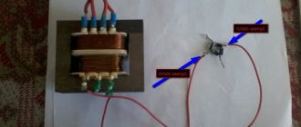
Now let's see in practice how this chip works. To do this, we will assemble the following circuit on a breadboard. This is more than enough to test its functionality.
We will power our design from an regulated power supply; we will set the output voltage to around 14-16 volts, which is quite enough. We will monitor the output voltages and signals using an oscilloscope.
We will monitor the output signal at pin 6 of the microcircuit. First, let's put the UC3843 chip on the breadboard and see how the sawtooth voltage generator works and what its output is. We connect the first beam of the oscilloscope to the MS output (pin 6), the second to the sawtooth voltage generator (pin 4). Move variable resistors down the circuit so that the operation of the microcircuit is not affected.
We see that with each pulse of the sawtooth voltage generator, there is one pulse at the output with a duty cycle of about 100% (several percent dead time). That is, the output frequency corresponds to the frequency of the generator. Let's now take the UC3845 chip and compare the output voltage with the 3843.
What do we see? For one output pulse there are two pulses of the sawtooth voltage generator. That is, the output frequency of this microcircuit will be half the frequency of the master oscillator. The duty cycle of the output pulses here is about 50%. Let's now see how current protection works. To do this, we connect the second beam to pin 3 of the microcircuit (the first at the MS output and the zero level of this beam at the second division from the bottom). The zero level of the second beam is at the bottom of the screen below the zero level of the first beam (the beam is at the level of one division).
We set the sensitivity of the second beam to 0.5 volts per division. At pin 3, there is no input voltage yet and there are pulses at the output (pin 6). We begin to increase the input voltage at pin “3”, simulating an increase in current through the output transistor.
What do we see? As soon as the input voltage at pin “3” reached a threshold of 1.0 volts (the beam rose by two divisions), the pulses stopped at the output of the microcircuit. Let's now see how the output voltage of the power supply is adjusted by the microcircuit. For this purpose, we will now connect the second beam to pin “2” of the microcircuit.
There is no input voltage at pin “2”. Pin “6” has output pulses. The sensitivity of the second beam (lower) is set to 1.0 volts per division, it is at the very bottom of the screen. We begin to slowly raise the input voltage at pin “2” of the microcircuit using a variable resistor until there is no change in the output. The lower beam began to rise upward.
What do we see? As soon as the input voltage at pin “2” rose to 2.5 volts, maybe a little higher (the lower beam rose up two and a half divisions), the output pulses at pin “6” stopped. Let's now see what will happen at the output of the error amplifier in the same situation, that is, at pin “1” of the microcircuit. We connect the second beam to pin “1”, set the sensitivity of the beam to 0.5 volts per division, and reduce the voltage at the input (pin “2”) again.
We turn on the power, the input voltage at pin “2” is minimal, at pin “1” the output voltage is around 2.5 volts (the lower beam is raised by five divisions). We begin to gradually increase the voltage at the “2” pin of the microcircuit using a variable resistor. The upper beam crawled down, that is, the voltage at pin “1” began to decrease. Using a variable resistor, we increase the input voltage at pin “2” even more until there are any changes in the output voltage at pin “6”.
That's it, the pulses at the output of the microcircuit have stopped, the first beam is at its zero mark (second division from the bottom), the voltage at pin “1” is about 0.7 volts (the second beam is raised a little more than one division from its zero line).
Now I will try to present everything that we have seen in practice theoretically below. In this microcircuit, voltage stabilization and current protection occur differently than in the TL494 microcircuit we previously reviewed. Here we will not see a smooth change in the width of the output pulses from changes in the input voltage at the input of the error amplifier (pin “2”), or at the input of the current comparator (pin “3”), since the output pulses of the microcircuit (output stage) are controlled by a comparator (current comparator ), and if any thresholds are exceeded, it simply turns off the output stage, and then, when the voltages and currents are normalized, it turns it on. The inverting input of this comparator is internally biased by 1.0 volts. Limitation (disabling) of output pulses occurs if this threshold of 1.0 volts is exceeded at pin “3” of the comparator, or if the voltage at pin “1” is reduced so that it does not exceed the voltage drop across two diodes connected in series (we succeeded about 0.7 volts). The voltage at this pin reaches this value if the input voltage at the input of the error amplifier (pin “2”) exceeds 2.5 volts, because a voltage of 2.5 volts is supplied to the non-inverting input of this error amplifier through internal circuits, that is, it looks like the TL-431 works. Pin “1” can also be used as a second circuit for regulating the output voltage, if, for example, a transistor controlled by an LED (optocoupler) is connected to this output, which is connected to the power supply output. You can also block (emergency shutdown) the microcircuit using this input by connecting it with a transistor or something else to the common wire.
To explain it in a more understandable language, the output voltage (current) is controlled here also by error amplifiers, as in the TL494, the only difference is that in the TL494 the duty cycle of the output pulses changes, but here the control occurs in bursts of output pulses. That is, when the power supply is turned on, pulses appear at the MS output. The voltage at the power supply output begins to increase, and when the set threshold is reached (for example, 12 volts), when the filter capacitor is charged to this voltage, the pulses at the MS output stop. The connected load consumes current and the capacitor discharges. The output voltage begins to decrease and at this moment (after a certain threshold) the MS is turned on and pulses are sent to the output again. After several pulses (a burst of pulses), the capacitor is again recharged to the set threshold and the pulses stop again. If the load current is small, then several pulses are enough to recharge the capacitor (a short burst) and, accordingly, more time passes for the next burst of pulses to be sent to the output (the distance between the bursts of pulses is greater). As the load current increases, a correspondingly greater number of pulses are needed in a burst (long burst) to charge the capacitor, and accordingly the time between bursts of pulses also decreases. If we imagine that a burst of pulses is one pulse (which can be narrower or wider), and the time (distance) between bursts is the time between each pulse, we get a complete analogue of PWM, just like TL494.
The output stage of the microcircuit is made according to a half-bridge circuit and is designed for an average current of about 200 mA, while the peak current can reach 1.0 A and at this level is limited by the microcircuit. The output stage can control both a powerful field-effect and a bipolar transistor.
Well, regarding these microcircuits, that’s basically all I wanted to say. There is a lot written about them on the Internet, and there is a lot of technical documentation. If you want to learn something more about them and in more depth, the search engine is in your hands.
Functional differences between microcircuits
For modifications of NCP1238B and NCP1288B microcircuits there are autorecovery support functions.
The NCP1237 has a dual-threshold OCP design, while the NCP1238 does not. The basic differences between the series microcircuits are shown in Table 3. Table 3. Basic differences between modifications of the NCP12xx series PWM controllers
| Modification | DSS | Dual OCP | Latch | Auto Recovery |
| NCP1237A | + | + | + | — |
| NCP1237B | + | + | — | + |
| NCP1238A | + | — | + | — |
| NCP1238B | + | — | — | + |
| NCP1287A | HV only | + | + | — |
| NCP1287B | HV only | + | — | + |
| NCP1288A | HV only | — | + | — |
| NCP1288B | HV only | — | — | + |
PWM controllers as part of power supplies
The power supply is an integral element of most modern devices. Its service life is practically unlimited, but the safety of the controlled device largely depends on its serviceability. You can design a power supply yourself by studying the principle of its operation. The main goal is to generate the required supply voltage and ensure its stability. For most powerful devices, galvanic isolation based on the action of a transformer will not be enough, and the selected element will clearly surprise users with its dimensions.
Increasing the frequency of the supply current makes it possible to significantly reduce the size of the components used, which ensures the popularity of power supplies operating on frequency converters. One of the simplest options for implementing power elements is a block diagram consisting of forward and inverse converters, a generator and a transformer. Despite the apparent simplicity of implementing such schemes, in practice they demonstrate more disadvantages than advantages. Most of the obtained indicators change rapidly under the influence of supply voltage surges, when the converter output is loaded, and even when the ambient temperature increases. PWM controllers for power supplies make it possible to stabilize the circuit, as well as implement many additional functions.
Components of power supply circuits with PWM controllers
A typical circuit consists of a pulse generator based on a PWM controller. Pulse width modulation makes it possible to manually control the amplitude of the signal at the output of the low-pass filter, changing the pulse duration or its duty cycle if necessary. The strength of PWM is the high efficiency of power amplifiers, especially audio, which in general provides the devices with a fairly wide range of applications.
PWM controllers for power supplies can be used in circuits with different powers. To implement relatively low-power circuits, it is not necessary to include a large number of elements in their composition - an ordinary field-effect transistor can act as a key.
PWM controllers for high-power power supplies can also have output switch controls (drivers). It is recommended to use IGBT transistors as output switches.