How a class AB amplifier works (Push Pull) 02/19/2021 19:52
Class AB is the type of amplifier that, until recently, was used in Hi-Fi equipment many times more often than any other. Now the threatening shadow of class D amplifiers is already hanging over it, occupying an increasingly large share of the Hi-Fi market, but for now class AB models are still in the majority and they are not going to give up so easily. In the AB class, both tube and transistor circuits can work, but if we talk about the absolute majority, the AB class is more likely associated with the era of transistor Hi-Fi.
Principle of operation
From the very designation of class AB, it is easy to conclude that this mode is a hybrid of class A and class B. We have already figured out how class A amplifiers work, but we did not have time to familiarize ourselves with class B, so we will start with it. And to begin with, let us remember the logic that guided the creator of the class A amplifier. In order to be able to reproduce both positive and negative half-waves using one active element, he applied a shift of the midpoint (quiescent current) to the middle of the working area of the lamp.
The creators of Class B amplifiers reasoned differently: “If one tube or one zero-bias transistor can reproduce only one half-wave of the signal, why not add another active element to the circuit, placing it in a mirror, to reproduce the other half-wave?”
This is quite logical, because in this situation both transistors operate with zero bias. As long as there is a positive half-wave at the input of the amplifier, one transistor works, and when the time comes to reproduce the negative half-wave, the first transistor is completely closed and the second one switches on instead. In the English version, this operating principle is called push-pull or, in Russian, “pull-push,” which in general describes what is happening very well.
When comparing Class B to Class A, the most obvious advantage is that in Class B, each wavelength covers the full operating range of the transistor (or tube), while in Class A, both half-waves are reproduced by a single active element. This means that a class B amplifier will be twice as powerful as a class A amplifier assembled using the same transistors.
The second, slightly less obvious, but very important advantage of class B is zero bias currents. When the input signal is zero, the current flowing through the transistors is also zero, which means that there is no wasted energy consumption, and the energy efficiency of the circuit is several times higher than in class A.
However, the main drawback of a class B amplifier follows from this same fact. The moment the transistor is turned on after a completely closed state is accompanied by a slight delay, therefore, when the sound signal passes the zero point, when one transistor has already closed, the second transistor does not have time to instantly pick up the baton, and in At this very transition point, small time delays occur.
In practice, this is expressed in the amplifier’s particular dislike for quiet music, as well as in poor transmission of microdynamics. And although history knows successful implementations of class B, for example, the legendary Quad 405, the problems of this operating mode have not gone away. The same 405 not only pleased with its energetic and muscular sound, but also had a clear tendency to paint a sound picture with large strokes, on a large scale, without wasting time on trifles.
In order to preserve all the advantages of class B and solve the problem of transient processes, the engineers resorted to a trick. They turned on both transistors with a bias, as is done in class A, but the bias value was chosen to be significantly smaller: so as to cover only those moments when the transistor is close to closing, thereby removing transient processes from the working area.
This allowed the class AB amplifier to quietly overcome the zero point, and also provided another extremely useful effect. When the signal amplitude is small, falling within the limits of the quiescent current bias, such an amplifier operates in class A and only when the amplitude goes beyond the bias value selected by the manufacturer does it switch to AB mode.
Differences between Push and Pull modes
In Push mode, we manually or script start the process of applying changes on the server (locally or remotely).
Local Configuration Manager (LCM) applies the configuration interactively. In Pull mode, the LCM agent itself on the server compares its configuration with the configuration published in the shared configuration repository according to a schedule. If there are changes, the configuration is copied locally and applied.
The pros and cons of both operating modes are quite obvious.
| Push | Pull | |
| + |
|
|
| – |
|
|
Setting resources is also slightly different for different modes.
As we remember, to use the resource you need to install it locally and on the server. When using Push mode, the administrator must first install all the necessary resources on the managed server and on the PC from which the configuration will be sent.
In Pull mode, the DSC agent on the managed server can independently install all the necessary resources from the Pull server; the administrator’s task is to place them on the Pull server. However, keep in mind that it is impossible to predict the application of the configuration in Pull mode, since the GPO is not a guaranteed delivery of settings.
pros
It makes sense to consider the advantages and disadvantages of the AB class against the backdrop of the two initial technologies. Class AB clearly and significantly outperforms class A in terms of energy efficiency. Its real efficiency reaches 70–80%, unless of course the manufacturer is too keen on raising the quiescent current. From a sound standpoint, Class AB is superior to Class A when the signal reaches high amplitude or high power is required. At the same time, at low volume levels, class AB is not inferior to ordinary class A, at least in theory. Compared to class B, class AB behaves much better at low volumes and is able to handle the quietest and most delicate moments in music, but at the same time retains almost the same power and strength at large dynamic bursts.
Having more power and better energy efficiency, class AB amplifiers are much less capricious when choosing acoustics. They do not require high sensitivity and are more easily compatible with complex crossovers used in multi-way speakers. It would be fair to say that the vast majority of passive speaker systems on the market today are designed to work with the average class AB transistor amplifier.
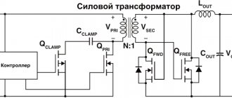
Power amplifier design method
The amplification path for nonlinear location devices must ensure operation in a mode close to the linear mode of operation of the amplifier in order to minimize the excitation of the harmonic components of the probing signal. Also, the amplification path must have sufficient stability and temperature stability to ensure the required service life of the product.
In order to solve the problem, it is proposed to take as a basis when designing a PA for nonlinear transition detection devices the topology of a push-pull power amplifier based on a GaN transistor.
Key benefits of using push-pull topology:
- Class A linear output can be achieved while achieving Class B amplifier efficiency, but using two GaN transistors instead of one;
- The push-pull topology assumes an ideal short circuit on the even harmonics of the main signal, which can significantly increase the efficiency of the PA when applied to problems of detecting nonlinear transitions.
However, there is a problem of achieving stability and efficiency of PAs made using a push-pull topology at frequencies above 2 GHz.
In Fig. Figure 1 shows the proposed block diagram of a PA using Push-Pull topology for use in devices for detecting nonlinear transitions.
Rice. 1. Structure of the Push-Pull topology PA
The proposed structure contains signal division/addition circuits with an output phase difference of 180° and output ports with an impedance of 25 Ohms, input/output matching circuits at 25 Ohms, an output circulator and low-pass filters for the gate and drain power supplies. The developed methodology proposes, instead of filter-based matching networks that limit amplifier performance for wideband applications, to use a simplified circuit topology based on the fact that the output impedance of the applied divide/add circuits with an output phase difference of 180°, amounting to 25 ohms, is close to transistor load resistance. The use of a circulator at the output of a power amplifier is necessary to reduce the influence of the antenna-feeder path on the output matching circuit of the power amplifier.
The next step, using a nonlinear amplifier model using the Load Pull method of variable loads, was to obtain the input and output impedances of the transistor at an output signal power of 10 W (40 dBm), on the basis of which the matching circuits were designed.
In Fig. Figure 2 shows the basic configuration for Load Pull modeling: source tuner at the input, load tuner at the output, T-couplers for supplying voltage bias to the gate and drain.
Rice. 2. Load Pull modeling scheme
The source matching simulation was carried out using the maximum output power in the case when the device output is loaded into 25 Ohms.
Obtained values of load and source impedance after simulation for the main signal frequency of 3950 MHz:
Zsource = 1.2 – j•8.1;
Zload = 3.8 – j•0.2.
The next stage was an electromagnetic simulation of the topology of the matching circuits in order to assess the influence of inhomogeneities of microstrip transmission lines, based on the results of which the input and output SCs were adjusted. The matching networks are designed to transform the 25 ohms input and output as closely as possible into the required source and load impedance, respectively. Also, when designing matching circuits, the RC circuit at the input was additionally taken into account to achieve transistor stability, which is recommended by the manufacturer Cree.
The matching circuit is shown in Fig. 3.
Rice. 3. Amplification stage matching circuit
The input matching circuit circuit contains a series-connected T-shaped power injector made in the form of a quarter-wave section of a microstrip line and a circuit for converting the impedance from 25 Ohms to the complex conjugate value of the Zsource impedance.
The output circuit is designed similarly to the input circuit: an impedance conversion circuit from the complex conjugate value of the load impedance Zload and a T-shaped power injector, made in the form of a quarter-wave section of a microstrip line, are connected in series.
In Fig. Figure 4 shows the developed circuit of the input matching circuit.
Rice. 5. Output matching circuit diagram
In Fig. Figure 5 shows the developed circuit diagram of the output matching circuit.
Rice. 5. Output matching circuit diagram
After electromagnetic simulation, the matching circuits were adjusted to adjust to the input and output impedance value of 25 Ohms. In Fig. Figure 6 shows the impedance values of the designed input and output matching circuits.
Rice. 6. Impedance of the designed input and output matching circuits after correction based on the results of electromagnetic simulation
As a signal division/adding circuit, it is proposed to use a coaxial transmission line with a length of λ/4 (Fig. 7), whose use allows reducing the cost of the final product and simplifying the PA topology.
Rice. 7. Signal division/addition circuit based on a λ/4 coaxial line and Smith chart of circuit simulation results [4]
In Fig. Figure 8 shows the resulting final topology of the printed circuit board of the power amplifier unit after adjustments to the input and output SCs.
Rice. 8. Topology of a power amplifier made according to the Push-Pull topology
After manufacturing, measurements of the characteristics of the PA, made according to the Push-Pull topology, were carried out.
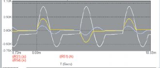
The table shows comparative characteristics measured for a Push-Pull topology PA and a classic Class A PA.
Minuses
The objective disadvantages of class AB can only be seen against the background of even more technically advanced classes G, H or D, which we will talk about a little later. The list of complaints can only include subjective reviews from class A connoisseurs, which, in general, boil down to the fact that class AB does not sound as clean, detailed and refined. To assess the validity of these claims, let's look at the circuitry of class AB amplifiers in more detail, from the point of view of sound quality.
Peculiarities
One of the practical problems of class B and AB amplifiers is the selection of pairs of transistors operating in the same amplification channel. Being positioned mirror-like in the circuit, the two transistors must be completely identical to each other. Otherwise, the signals of the positive and negative half-waves will not be reproduced symmetrically, and this will significantly increase the overall level of distortion.
In real life, absolute identity is an abstract concept; it makes more sense to talk about the degree of similarity or, in technical language, about the limits of permissible deviations of transistors from given characteristics. The more similar two transistors are to each other, the lower the level of distortion, and the more their joint work approaches what we have in class A, when both half-waves are reproduced by one transistor.
Understanding that even with the most stringent selection of parameters, differences between two transistors in a pair will still occur (albeit in extremely small values), we are forced to admit that, other things being equal, one of the same transistor operating in class A will sound slightly cleaner and slightly better than a pair in class AB.
A completely different situation emerges when it comes to working with a large signal amplitude and a load requiring high power. Having high efficiency, class AB requires a less powerful and bulky power supply than a class A amplifier, and here fans of single-ended amplifiers are forced to admit the absolute and unconditional superiority of class AB.
Moreover, developers have the opportunity to experiment much more freely with power supplies, controlling the character and dynamics of the sound by selecting the operating characteristics of the transformer and capacitors. For example, you can install a transformer with multiple power reserves so that during signal peaks it does not leave the optimal operating mode, or use improved capacitors that can instantly deliver high current.
Another subtlety: when operating in class A, transistors generate a large amount of heat, which can negatively affect the quality of their work, especially when the load increases. In class AB, transistors heat up to a lesser extent, as a result of which they quickly return to operating mode and are less susceptible to the risk of overheating, which reduces sound quality when the amplifier operates at high volumes.
Hello student
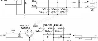
Push-pull converters can be self-excited or independently excited. Currently, converters with independent excitation, which have a higher efficiency, are mainly used. In practice, three main circuits of push-pull converters are used: with the output of the neutral point of the primary winding of the transformer (with a midpoint), half-bridge and bridge. The transformer included in the converter has two identical primary windings with the number of turns W11 = W12 = W1 and two identical secondary windings with the number of turns W21 = W22 = W2.
Let us consider the steady-state operating mode of an ideal converter in the case of continuous inductor currents L with pulse-width control of transistors VT1 and VT2. When the control transistor VT1 is switched to saturation mode, the energy source voltage U0 will be applied to the primary winding W11 of the transformer.
As a result, an EMF E2 will appear at the terminals of the secondary winding W21 with a polarity that ensures the opening of the diode VD1. In this case, during the open state interval VT1, all other diodes and transistor VT2 will be closed.
Since EMF E2 = U0n21 = U0W2/W1, a voltage equal to U0n21 - Un will be applied to the inductor winding L. Under the influence of this voltage, the current in the inductor winding L will increase linearly from the minimum to the maximum value corresponding to the moment of time t = γT, when the control system switches the transistor VT1 to the closed state.
During this time interval, energy is transferred to the load, energy is accumulated in the inductor L, and capacitor C1 is recharged. In this case, the voltage applied to the closed transistor VT2 turns out to be equal to 2U0. When the transistor VT1 is turned off, the polarity of the EMF changes at the terminals of all windings of the transformer, which leads to the blocking of the diode VD1 and the opening of the diode VD3. As a result, a voltage equal to the voltage on the load will be applied to the inductor winding, and it will transfer previously stored energy to the load and capacitor C1 (as long as the inductor current is greater than the load current). In this case, the voltage applied to the closed transistors VT1 and VT2 turns out to be equal to the voltage of the energy source U0, since the transformer is in short circuit mode (with the primary winding disconnected from the energy source).
At the moment t/T = 0.5, the control system switches transistor VT2 to the open state, as a result of which the primary winding W12 of the transformer (which is in short circuit mode) is connected to the energy source. This leads to a sharp increase in current in the windings W22 and W12 of the transformer. At the moment when the current in winding W22 reaches the value of the inductor current L, the process of blocking the diode VD3 begins. In the interval 0.5T ≤ t ≤ (0 5 + γ)T, transistor UT2 is open and in saturation mode, and the inductor current again increases from the minimum to the maximum value.
The control characteristic of this converter has the following form: UH = 2n21γU0.
As can be seen from the expression, the regulating characteristic of this converter differs from the regulating characteristic of a single-stroke converter with direct connection of a diode only by a factor of 2. However, in the latter case, two separate transformers are required, the calculated power of each of which is half the power of the transformer of the push-pull converter. In addition, it should be remembered that the magnetization reversal of the magnetic core material in single-ended converters with direct connection of the diode is carried out according to a partial asymmetrical magnetization reversal cycle, whereas in this ideal converter the magnetization reversal is carried out according to a partial symmetrical cycle. Therefore, the dimensions of the transformer in a push-pull converter will be smaller compared to the dimensions of the two transformers of single-stroke converters.
The expression for the critical value of the inductance Lcr of the inductor L, which ensures continuity of the inductor current at a minimum value of the load current Jн min, takes the following form for a push-pull converter (or two single-cycle converters operating on a common filter):
The difference in operation will only be that during the intervals of the closed state of the transistors, both diodes at the output of the converter (VD1, VD2) will be open and a current equal to half the inductor current will be closed through each of them. For example, booster (stabilizing) converters KV-12/100 (KS-14/100), widely used in power supply systems for telecommunications equipment, are the considered push-pull converter in the version without the VD3 diode.
In real push-pull converters operating at frequencies of 20 kHz and higher, the unequal value of the absorption time of excess carriers in transistors when they are turned off leads to the fact that the increment of magnetic flux in the transformer in the open state interval of one transistor differs from the magnetic flux increment in the open state interval of the other transistor. As a result, in push-pull converters, so-called one-sided magnetization of the transformer magnetic core material may appear. And, as a result, saturation of the magnetic circuit material and a short circuit for the energy source, leading to failure of the transistors. Another reason for the appearance of one-way bias is the electrical asymmetry of the circuit, which usually occurs at low output voltage levels. In order to eliminate the phenomenon of one-sided magnetization, it is necessary to resort to a significant complication of the control circuit in push-pull converters compared to single-cycle converters. For this purpose, for example, a device is introduced into the control circuit that monitors the average value of the transistor currents and, when they are unbalanced, provides automatic correction of the duration of the transistors' on state.
The considered converter is used in practice at relatively low voltages of the energy source, since the voltage applied to a closed transistor is twice the voltage of the energy source. At high voltage U0 (several hundred volts), half-bridge and bridge circuits of push-pull converters are widely used.
In a half-bridge converter, two capacitors with the same capacitance are installed in parallel with an energy source with voltage U0. The primary winding of transformer TV1 is connected between the common point of these capacitors and the common point of transistors VT1 and VT2.
In an ideal converter, the average voltage across each capacitor is equal to half the voltage U0. When the control system, for example, transistor VT1, is transferred to saturation mode, the voltage applied to the primary winding of transformer TV1 will be equal to the voltage on capacitor C1. As a result, the EMF E2 at the terminals of the secondary winding VT1 will be equal to U0n21/2. In this case, diodes VD3 and VD6 will be open. The voltage applied to the closed transistor VT2, equal to the sum of the voltage on the capacitor C2 and the emf of the primary winding TV1, will be equal to the voltage U0. In order to exclude intervals during which both transistors are open simultaneously, the duration of the open state of VT1 and VT2 must be less than half the energy conversion period. During open state intervals VT1 (VT2), energy is transferred to the load and accumulated in inductor L1 and capacitor C3. The curves of the transistor collector current, inductor current L1, voltage at the input of filter L1 C3 and voltage at the load completely coincide in shape with the corresponding curves. During the off-state intervals of the transistors, all four diodes of the output rectifier are open and a current equal to half the inductor current flows through each of them, while the voltage applied to the closed transistors is equal to U0/2. The control characteristic of a half-bridge converter (when operating in the mode of continuous currents of inductor L1) has the following form: UH = γU0n21.
The expression for the critical value of the inductance Lcr of the inductor L, which ensures the continuity of the inductor current at the minimum value of the load current In min, takes the following form for a half-bridge converter:
Half-bridge converters are usually used with output power up to several hundred watts, since with increasing output power the overall dimensions of capacitors C1, C2 sharply increase. In addition, all other things being equal, the collector current of transistors in half-bridge converters is twice as large as in bridge converters, which leads to large losses in them and to an increase in the size of transistor cooling radiators.
In a bridge converter with the classical, so-called symmetrical method of controlling transistors, the control system ensures synchronous switching of diagonal transistors (VT1 and VT4 in the interval of the first half of the period, and then VT2 and VT3 in the interval of the second half of the energy conversion period). In this case, in the open state interval of any pair of diagonal transistors, the voltage applied to the primary winding TV1 and to each of the closed transistors in an ideal converter is equal to the voltage of the energy source. Otherwise, the operation of a bridge converter with a symmetrical method of controlling transistors is similar to the operation of the push-pull converters discussed above.
As the operating frequency of the converter increases, in the case of a symmetrical method of controlling transistors, the losses in the transistors when they are turned on also increase. This is due to the fact that the transistors are switched on (transferring them to saturation mode) at high voltages across them. Therefore, quite a lot of energy is stored in the parasitic output capacitances of the transistors (drain-source capacitance of the transistor), which is released on the transistors when they are turned on. So, at a supply voltage level U0 = 600 V (this voltage level, for example, may be the case when using a converter in a three-phase rectifier with a transformerless input), each of the closed transistors of the bridge converter will have a voltage Uci = 300 V. In this case, with the output capacitance drain-source Csi = 300 pF and the operating frequency of the converter ƒ = 300 kHz, the average power Rsi over the period, lost in the transistor when it is turned on, turns out to be equal to Wƒ = CsiU2ciƒ/2 = 300 • 10-12 • 3002 • 300 • 103/2 = 4.05 W. Consequently, power equal to 16.2 W is lost on four transistors of the bridge converter. The use of a phase method for controlling the transistors of a bridge converter makes it possible to ensure that its transistors are turned on at zero voltage across them, i.e., to eliminate losses in them when turned on. The essence of the phase method of controlling transistors is explained using timing diagrams uzii presented in Fig. 1 In the diagram of Fig. 1, and shows the output capacitances of transistors C1...C4 and diodes VD1...VD4, inherent in the structure of field-effect transistors. The numbering of the listed elements corresponds to the numbering of transistors. A choke L is introduced into the circuit of the primary winding of the TV transformer. As follows from the timing diagrams uzii (the index i takes values corresponding to the numbers of transistors in the circuit), the transistors forming the left (VT1, VT2) and right (VT3, VT4) “racks” are switched on in in antiphase with a short delay trear of turning on one transistor relative to the moment of turning off the other transistor of this rack. This delay is necessary to prevent the simultaneous opening of both transistors of one rack, which is a short circuit for the energy source U0. Moreover, the duration of the open state of each of the four PN transistors is unchanged and close to half the energy conversion period. Regulation (stabilization) of the output voltage (voltage on RH) is carried out due to the phase shift of the front of the turning-on pulses of the transistors of one rack relative to the turning-on pulses of the transistors of the other rack.
In the interval [0, t1], diagonal transistors VT1 and VT4 are open, as a result, current i1, equal to the sum of the magnetizing current (no-load current) of the transformer and the inductor current: L1, reduced to the primary winding, flows into the beginning of the primary winding TV, the output diode is open VD5 and energy is transferred to the load and accumulated by chokes L1 and L. At the same time, the voltage is on capacitors C2 and C3. equal to voltage U0. At moment t1, the control circuit turns off VT4, as a result of which current i1 begins to close in the circuit: primary winding TV (in the same direction) - capacitor C3 - open transistor VT1 - inductor L. The rapid process of recharging capacitor C3 and charging capacitor C4 begins. In a time less than tset, the voltage on capacitor C3 decreases to zero, and on capacitor C4 increases to U0. After the voltage on C3 has dropped to zero, the diode VD3 opens and the current i1 is further closed through this diode, so that by the moment t2 - the moment VT3 opens - the voltage on it is practically zero, i.e. there are no power losses when it opens. In the interval [t2, t3], the primary winding TV and inductor L are short-circuited by diode VD3 and transistor VT1, so that the current in this circuit undergoes virtually no change. At moment t3, transistor VT1 turns off and capacitor C2 quickly recharges (and capacitor C1 charges), so that in a time less than tset, the voltage on C2 drops to zero, after which diode VD2 opens. Until moment t4—the moment transistor VT2 opens—the current maintained by inductor L is closed through diodes VD2, VD3 and the energy source U0, i.e., the energy stored by this inductor returns to the source. VT2 is also switched on without loss of power. In the interval [t4, t5], VT2 and VT3 are open, current i1 changes its direction, the output diode VD6 is open and energy is transferred from the source to the load, and is also stored in chokes. Further processes in the circuit proceed in a similar way.
To eliminate the phenomenon of one-sided magnetization of the transformer in half-bridge and bridge voltage transformers, a capacitor is often switched on in series with the primary winding of the transformer. Such introduction of a capacitor takes place, for example, in the PN of PC power supplies, in the VBV-60/25-3k rectifiers.
At the output of any of the considered push-pull converters, the output rectifier can be made either using a single-phase bridge circuit or a full-wave rectification circuit. A single-phase bridge rectification circuit is usually used only at relatively high output voltage levels (several tens of volts or more), as it is characterized by large losses in the valve set compared to a full-wave circuit.
Literature used: Power supply of devices and telecommunication systems: Textbook for universities / V. M. Bushuev, V. A. Demyansky, L. F. Zakharov, etc. - M.: Hotline-Telecom, 2009. - 384 pp.: ill.
Download abstract: You do not have access to download files from our server. HOW TO DOWNLOAD HERE
Archive password: privetstudent.com
Practice
Defending the honor of class AB amplifiers in comparative listening was destined to the powerful two-block amplifier Atoll Signature series, consisting of an AM200 power amplifier and a PR300 preamplifier. The power amplifier we are interested in is built in full accordance with the theoretical calculations outlined above.
Realizing the potential inherent in class AB circuitry, the developers have provided 120 W of output power per channel, which is enough for most speaker systems except the most low-sensitive and simply monstrous models. Speaking about the features of its amplifier, the manufacturer focuses on the use of selected pairs of transistors, followed by manual adjustment of the circuit to minimize the overall level of distortion.
In order to better separate the channels and eliminate crosstalk, the amplifier is built according to a full dual mono circuit, so each amplification channel has its own power supply. The total power of the power supply is 670 VA, which covers the needs of a 120 W amplifier with a large margin. Solid additional power at signal peaks will be provided by capacitors with a capacity of 62,000 μF.
Introduction
The classic method for detecting hidden microelectronic devices containing working or non-working elements with a nonlinear current-voltage characteristic is the method of emitting a polarized electromagnetic wave of a monochromatic (single-frequency) signal and receiving the second and third harmonic components of the echo signal. The emitted signal is amplitude modulated, and at the receivers the dependence of the amplitude of the response signal on the amplitude of the probing signal is measured, which provides additional information about the type of nonlinearity. The key problems of this approach are considered to be a short detection range due to the influence of the harmonics of the emitted signal on the receiver input, as well as the impossibility of determining the type of detected device due to insufficient input data. One of the modern approaches in the field of detection of nonlinear transitions is a probing method using broadband modulated radiation with a central frequency fc, band BW and the implementation of reception and digitization using high-speed ADCs of the echo signal at central frequencies 2fc and 3fc. The use of broadband modulated radiation allows, in addition to obtaining the dependence of the radiation power on the amplitude of the echo signal, to also measure nonlinear distortions of the received modulated echo signal, which significantly expands the possibilities of subsequent analysis to determine the type of detected device. Research also shows that the use of broadband radiation can increase the detection range of hidden electronic devices. However, the development of this kind of high-performance devices for detecting nonlinear transitions requires a more complex configuration of both the high-frequency amplification path of the transmitting signal and the antenna-feeder system:
- the requirements for the operating bandwidth of the amplifier are increasing;
- the requirements for linearity of the amplifier operation are increased;
- it is necessary to develop PA taking into account nonlinear distortions, due to the use of a wideband modulated signal;
- Due to the specific nature of devices for detecting nonlinear transitions, it is also necessary to minimize the level of harmonic components of a broadband signal.
Taking into account all of the above, designing an amplifier stage becomes one of the most key tasks in the development of this type of device.
In the field of constructing output power amplifiers, it is to some extent limited by the lack of a sufficient range of electronic components with the necessary power parameters. Silicon and gallium arsenide high-power microwave transistors have almost reached their limit due to limitations in the electrophysical parameters of the original semiconductor materials. For the creation of microwave electronic components and high-power output devices, the advantages of gallium nitride technology, which are reflected in previously conducted studies, are especially important [1, 2].
This paper presents the results of applying a methodology for designing a broadband large-signal push-pull power amplifier based on GaN components for high-performance nonlinear transition detection devices. The technique reflects solutions to the problems of convergence of design results when developing a Push-Pull topology PA. Comparisons of two different PA topologies are presented to compare their characteristics.
Sound
The impressive power and excellent energy efficiency of the amplifier gave the sound the expected feeling of lightness and ease when working with any acoustics and at almost any volume level. If you turn the volume knob up, you can hear a little compression and the bass seemed to take a backseat, but these were clear signs that the woofers were nearing their limits, while the amp was just starting to warm up and was very far from being overload.
At the same time, the Atoll AM200 Signature performed best at low and medium volume levels. The midrange was expressive, detail was excellent, and the stage was clearly defined, with well-perceived depth and width. In direct comparison with Class A amplifiers, the latter gave a slightly freer and more limitless stage and worked out fine details in quiet chamber music a little more subtly.
The character characteristic of the AB class was most clearly manifested in the Atoll AM200 Signature on dynamic rock music. It produced very focused, fast and clear bass, handling sudden volume changes and large strokes well. On jazz and classical music, which require a combination of dynamics and power with the ability to reproduce subtle shades and nuances, the amplifier behaved a little less confidently. It seemed that he was slightly simplifying the sound, enlarging the musical images and drawing attention away from subtle shades to the main melodic line.
However, all this can only be noticed in direct comparison with much more expensive representatives of other classes. The overall impression was that the Atoll AM200 Signature was rather omnivorous and versatile. Being an example of a competent implementation of the AB class, when the developers made a lot of effort to minimize weak points and maximize the potential of this circuit design, it is quite competitive against the background of the best representatives of other classes.
conclusions
High power, high efficiency with moderate heat dissipation, the ability to cope with complex loads and good dynamics - this is what an AB class amplifier is. This makes it, first of all, an ideal solution for mass production of amplifiers, as confirmed by the very history of the development of the Hi-Fi industry.
However, it is extremely erroneous to be guided by the stereotypical opinion that a mass universal product and an elite product must necessarily be molded from different cloth. With proper attention to detail and a deep understanding of operating principles, this circuit design can be implemented at the highest level of quality. So today, a high-end amplifier operating in class AB is as commonplace as a high-end amplifier operating in any other circuit design.
https://stereo.ru/