December 17, 2019
resource accountingpower managementconsumer electronicsautomationinternet of thingsMaxim Integratedarticleintegrated circuitsdevelopment tools and materialsDC-DC
Alexander Rusu (Odessa)
The overall efficiency of a pulse converter self- powered low-power electronic devices is reduced mainly due to the leakage current of the control circuit. Integrated DC/DC from the new nanoPower produced by Maxim Integrated will help reduce this current to almost zero .
Today, finding or making your own high-quality DC-DC converter with a power from several watts to several kilowatts is not particularly difficult. However, powering equipment whose power consumption is measured in microwatts is already a serious technical problem, because at such consumption levels the relative amount of “overhead” in the form of energy consumption for operating the control circuit increases, which leads to a noticeable decrease in the efficiency of the converter as a whole. In addition, almost all modern battery-powered devices actively use energy-saving modes, in which all currently unused systems are disconnected from the energy source. And this further tightens the requirements for power supplies, because now they must also have the minimum possible leakage current when turned off.
At the same time, the number of battery-powered devices is constantly increasing every year, and the requirements for them are becoming more stringent. Therefore, most leading manufacturers of electronic components regularly offer engineers new solutions in this area.
Maxim Integrated , which not so long ago introduced a line of nanoPower , did not stand aside . Today, this line contains low-power operational amplifiers, comparators, temperature sensors and other components that are actively used in a wide variety of radio devices. Of course, Maxim Integrated did not ignore the sector of DC/DC voltage converters, having developed entire families of specialized microcircuits with ultra-low power consumption within this area.
Comparison of linear and pulse conversion methods
The most popular DC voltage converter circuit can be called a step-down one, because in real equipment the task of reducing voltage arises much more often than increasing or changing its polarity. But you can reduce the input voltage in two ways: pulsed and linear. Since each method has its own advantages and disadvantages, and therefore its own areas of application, the developer needs to study them.
The fundamental difference between linear and pulsed voltage reduction methods can be understood from Figure 1. A linear stabilizer operates on the principle of a resistive voltage divider. Its regulating element (transistor VT1) operates in active mode, providing such a voltage drop between the collector and emitter terminals that the output voltage VOUT at the RLOAD load is within the specified limits. Since the entire load current IOUT flows through transistor VT1, the efficiency of this circuit will directly depend on the voltage difference between the input and output (formula 1):
$$\eta =\frac{P_{OUT}}{P_{IN}}=\frac{I_{OUT}\times V_{OUT}}{I_{OUT}\times V_{IN}}=\frac{ V_{OUT}}{V_{IN}},\qquad{\mathrm{(}}{1}{\mathrm{)}}$$
where PIN and POUT are the input and output powers of the converter, respectively.
Rice. 1. Comparison of linear and pulsed voltage reduction methods
And now the main drawback of linear stabilizers becomes obvious - the greater the voltage difference between the input and output, the lower its efficiency, and almost all the “extra” power is allocated to the VT1 control element, which requires installing it on a radiator, the dimensions of which sometimes exceed the dimensions of all others device elements.
Until recently, linear stabilizers were built on the basis of bipolar silicon transistors, most of which had a voltage drop between the collector and the emitter physically could not be less than 1 V. For stabilizers with a relatively high output voltage (more than 5 V), such a voltage drop was still quite acceptable, however, in modern microcontroller devices whose supply voltage can be less than 1 V, the use of bipolar transistors in this mode is unacceptable.
At one time, this led to the creation of linear stabilizers using field-effect transistors as regulating elements, which, as is known, do not have such a limitation. These stabilizers in Russian-language literature are called “low-dropout voltage stabilizers”, or LDO stabilizers/regulators (Low-Drop Out Regulator). Since, with a small voltage difference between the input and output, the efficiency of LDO stabilizers is not inferior to pulse converters, and their weight, dimensions and level of electromagnetic interference are much smaller, they are still actively used in modern technology.
In pulse converters, the active mode of semiconductor components is not used in principle. In the example under consideration (Figure 1), transistor VT1 operates in switching mode, periodically connecting the load RLOAD to the power source for a time tON. This means that the power release on power semiconductor components can theoretically be as small as desired and does not depend on the voltage ratio between the input and output, which is the main advantage of these circuits. Unfortunately, this conversion method also produces the main disadvantage - the pulsating nature of the output voltage with a high content of high-frequency harmonics.
Since it is not possible in most cases to use such voltage to power consumers, filters must be installed at the output of pulse converters to reduce output voltage ripple. Moreover, these filters must necessarily use reactive elements capable of storing energy (an active filter based on semiconductor transistors is not suitable for this purpose). This means that a pulse converter simply physically cannot be miniature, because the energy capacity of reactive components is directly proportional to the mass and volume of the magnetic or dielectric material used in them.
If we compare the advantages and disadvantages of linear and pulse converters (Table 1), it turns out that they mutually compensate each other. Therefore, in practice, hybrid systems are very often used: a pulse converter generates some intermediate voltage of low stability with a relatively high ripple level, and the final fine adjustment is already carried out using linear LDO stabilizers.
Table 1. Comparison of pulse and linear conversion methods
| Method | Pulse | Linear |
| Ratio of input and output voltage | Any | The output voltage cannot be greater than the input voltage |
| Output voltage stabilization accuracy | Due to the fact that energy is converted in “portions”, the accuracy of the output voltage depends on the nature of the transient processes and the stabilization method | Theoretically unlimited. Practically determined by the noise level and stability of the characteristics of the components used |
| Output voltage ripple level | High. When using some control methods (hysteresis), it fundamentally cannot be low | Theoretically, it can be as small as desired. Almost limited by the performance of the components used |
| Electromagnetic interference level | High due to high rates of change in voltages and currents | Theoretically, it can be arbitrarily small |
| Efficiency | High | Determined by the voltage difference between input and output |
| Weight and dimensions | Depends on the conversion frequency. Typically larger than linear converters | Depends on the level of power dissipation. At low powers they can be microscopic |
| Circuit complexity | Complex | Relatively simple |
| Price | Relatively high | Low |
| Main scope of application | Converters with high input-to-output voltage ratio, current type converters, multi-channel converters and others | Stabilizers for components requiring precision output voltage with low ripple and electromagnetic interference |
In modern equipment, linear converters are primarily used to power low-power components that require high-quality, low-ripple output voltage, as well as in applications sensitive to electromagnetic interference, and switching converters in all other cases (where possible).
However, linear converters have one serious drawback, which in some cases makes their use impossible - the output voltage of a linear converter fundamentally cannot be greater than the input voltage. This means that in cases where the voltage needs to be increased or its polarity changed, the pulse conversion method has practically no alternative.
Introduction
In recent years, electronic component manufacturers have increasingly used contract manufacturing of semiconductor devices. Such companies employ highly qualified specialists - developers and circuit designers, and the production of finished products is located in the world's best factories, equipped with the most modern equipment. This is due to the obvious benefits that the development company receives:
- a sharp reduction in overhead costs associated with maintaining our own high-tech production;
- the ability to select the best contract manufacturers to ensure high quality products;
- focusing efforts on developing new products and technologies;
- guarantee of a long life cycle of devices;
- high production dynamics, as a result - low delivery times for products to end consumers;
- relatively low number of employees and at the same time high professional level.
All this makes it possible to significantly reduce the cost of products and, as a result, the price for the end consumer, while ensuring high quality and advanced circuit solutions.
A prime example of such a company is Monolithic Power Systems (MPS). MPS was founded in 1997 in Santa Clara (USA). Currently, the company employs about 100 people, among its investors are Bank of America, Investar, Aser Venture. Holding 18 patents in the field of BiCMOS and DMOS technologies, the company specializes in the design and contract manufacturing of power integrated circuits for DC power supplies, solid-state light sources, cold cathode fluorescent lamp drivers and Class D audio amplifiers. In the future, MPS plans to develop integrated network controllers power supplies. Advanced technology solutions enable the integration of digital control circuits, precision analog components and power transistors on a single chip, achieving high power densities in ultra-small integrated circuit sizes.
This article will review a line of integrated circuits for DC power supplies.
Operating principle of pulse converters
Today, there are many pulsed-DC voltage converters, differing in the number and type of reactive components, conversion algorithms and other characteristics. However, the simplest, and therefore the most popular, are only four circuits: buck, boost, inverting and flyback (Figure 2). These converters use the same operating principle, have an identical number of components and differ only in the method of switching the storage choke L1, on the operating mode of which all the characteristics of the circuit depend.
Rice. 2. Circuits of the most popular converters
The conversion of electrical energy occurs in two stages. At the first stage, the switch S1 is closed, and a certain voltage VL1 is applied to the inductor L1, under the influence of which, during the time tON, its current increases by the amount dI1 (formula 2, Figure 3):
$$dI_{1}=\frac{V_{L1}}{L_{1}}\times t_{ON},\qquad{\mathrm{(}}{2}{\mathrm{)}}$$
where L1 is the inductance of the winding active in the first stage.
In this case, a voltage of reverse polarity is applied to the diode VD1, so no current flows through it. At the end of this interval, the inductor current reaches the maximum value IMAX1, which means that energy E accumulates in its magnetic circuit (formula 3):
$$E=\frac{I_{MAX1}^2\times L_{1}}{2}\qquad{\mathrm{(}}{3}{\mathrm{)}}$$
Rice. 3. Diagrams of inductor voltage and current of various converters
Since at the first stage the energy in the choke increases, it is often called the stage of accumulation or charging of the choke.
After opening the switch S1, a self-induction EMF is formed at the terminals of all windings of the inductor, the polarity of which is opposite to the polarity present at the first stage, this means that the inductor L1 now becomes not a consumer, but a source of electrical energy. Changing the polarity of the voltage on the windings leads to the opening of the diode VD1, which provides the path for current flow in the second stage, called the return stage, or inductor discharge.
Since the amount of energy in the inductor at the moment of switching the keys does not change, the current in its active winding immediately after opening the key S1 will also be maximum, but its value IMAX2 may change, because it can now flow through a different number of turns (formula 4):
$$E=\frac{I_{MAX2}^2\times L_{2}}{2},\qquad{\mathrm{(}}{4}{\mathrm{)}}$$
where L2 is the inductance of the winding active in the second stage.
The buck, boost and inverter choke usually contains only one winding, so L1 = L2, and therefore IMAX1 = IMAX2 = IMAX. But for a flyback circuit, the inductances L1 and L2 most often differ, so the current IMAX2 can be determined (formula 5) by equating formulas 3 and 4:
$$I_{MAX2}=I_{MAX1}\times \sqrt{\frac{L_{1}}{L_{2}}}=I_{MAX1}\times \frac{N_{1}}{N_{2 }},\qquad{\mathrm{(}}{5}{\mathrm{)}}$$
where N1 and N2 are the number of turns, respectively, of the primary and secondary windings.
The second part of formula 5 can be easily obtained by remembering that the inductance of the winding is proportional to the square of the number of turns (formula 6):
$$L_{1,2}=N_{1,2}^2\times A_{L},\qquad{\mathrm{(}}{6}{\mathrm{)}}$$
where AL is the design parameter of the magnetic circuit.
After the diode opens, the voltage on the inductor winding is fixed at the level VL2, under the influence of which the inductor current during the time tOFF will decrease by the amount dI2 (formula 7):
$$dI_{2}=\frac{V_{L2}}{L_{2}}\times t_{OFF}\qquad{\mathrm{(}}{7}{\mathrm{)}}$$
In a quasi-steady state, when there are no transient processes in both the power and load circuits, the inductor at the second stage of conversion must release all the energy accumulated in the first interval. This means that by the time the next cycle begins, its current should be the same as at the beginning of the previous one. For circuits with a single-winding inductor dI1 = -dI2, but in the general case (for a flyback converter), changes in winding currents are determined by the Total Current Law (formula 8):
$$dI_{1}\times N_{1}=-dI_{2}\times N_{2}\qquad{\mathrm{(}}{8}{\mathrm{)}}$$
Substituting ratios 2 and 7 into formula 8, taking into account 6, we can obtain the basic equation 9, which relates the voltage values at the terminals of the inductor windings with the ratio of the durations of the main stages of the conversion:
$$\frac{V_{L1}}{N_{1}}\times t_{ON}=-\frac{V_{L2}}{N_{2}}\times t_{OFF}\qquad{\mathrm{ (}}{9}{\mathrm{)}}$$
Formula 9 is the basis for obtaining the regulating characteristics of the converter - the dependence of the output voltage on the relative duration of the first stage of conversion D = tON/(tON + tOFF). However, in order to obtain these dependencies, it is further necessary to consider each scheme separately.
Power supply for powering portable and pocket receivers
The transformerless power supply (Fig. 23) is designed to power portable and pocket receivers from an AC mains voltage of 220 V. It should be taken into account that this source is not electrically isolated from the supply network. With an output voltage of 9V and a load current of 50 mA, the power supply consumes about 8 mA from the network.
Rice. 23. Scheme of a transformerless power source based on a pulse voltage converter.
The mains voltage, rectified by the diode bridge VD1 - VD4 (Fig. 4.23), charges capacitors C1 and C2. The charging time of capacitor C2 is determined by the circuit constant R1, C2. At the first moment after turning on the device, thyristor VS1 is closed, but at a certain voltage on capacitor C2 it will open and connect circuit L1, NW, to this capacitor.
In this case, capacitor S3 of large capacity will be charged from capacitor C2. The voltage on capacitor C2 will decrease, and on SZ it will increase.
The current through inductor L1, equal to zero at the first moment after opening the thyristor, gradually increases until the voltages on capacitors C2 and SZ are equalized. As soon as this happens, the thyristor VS1 will close, but the energy stored in the inductor L1 will for some time maintain the charge current of the capacitor SZ through the opened diode VD5. Next, the diode VD5 closes, and the relatively slow discharge of the capacitor SZ through the load begins. Zener diode VD6 limits the voltage across the load.
As soon as the thyristor VS1 closes, the voltage on capacitor C2 begins to increase again. At some point, the thyristor opens again, and a new cycle of operation of the device begins. The opening frequency of the thyristor is several times higher than the voltage pulsation frequency on capacitor C1 and depends on the ratings of the circuit elements R1, C2 and the parameters of the thyristor VS1.
Capacitors C1 and C2 are MBM type for a voltage of at least 250 V. Inductor L1 has an inductance of 1...2 mH and a resistance of no more than 0.5 Ohm. It is wound on a cylindrical frame with a diameter of 7 mm.
The winding width is 10 mm, it consists of five layers of PEV-2 0.25 mm wire, wound tightly, turn to turn. An SS2.8x12 tuning core made of M200NN-3 ferrite is inserted into the frame hole. The inductance of the inductor can be varied within wide limits, and sometimes even eliminated completely.
Buck converter
A Step-Down Converter (Buck Converter) usually has only one winding, so N1 = N2. At the first stage of conversion, the difference between the input and output voltages (VL1 = VIN - VOUT) is applied to the inductor, and at the second - only the output voltage (VL2 = VOUT), as shown in Figure 4. Substituting these values into formula 9, we obtain formula 10:
$$\left(V_{IN}-V_{OUT} \right)\times t_{ON}=-V_{OUT}\times t_{OFF}\qquad{\mathrm{(}}{10}{\mathrm {)}}$$
Therefore (formula 11):
$$V_{OUT}=V_{IN}\times \frac{t_{ON}}{t_{ON}+t_{OFF}}=V_{IN}\times D\qquad{\mathrm{(}}{ 11}{\mathrm{)}}$$
Rice. 4. Operating principle of a buck converter
Equation 11 shows that the output voltage VOUT of the buck converter cannot exceed the input voltage VIN, otherwise the left side of the equation will become negative, a unipolar voltage will be applied to the inductor at both stages of the conversion, and the circuit will not work.
Chapter 4 - Code to Control the Converter
Since I will talk about control algorithms in a separate article, today the converter will be controlled by the same program that was used in the article that talked about the buck topology, you can read it here.
In the code chapter you can read in detail about the initialization of HRPWM and ADC, as well as their synchronization. Changes in the code occurred only in one place, namely in the interrupt handler with the ADC - the cutoff threshold changed, because I used a different voltage divider. Well, I corrected the condition so that there was no excessive overshoot:
void ADC1_2_IRQHandler (void) { ADC2->ISR |= ADC_ISR_EOC; adcResult = ADC2->DR; if (adcResult >= 3400) { dutyControl = dutyControl - 10; } else { dutyControl = dutyControl + 10; } SetDutyTimerA(dutyControl); } You will find the original project for TrueSTUDIO at the end of the article in archive form. Now that the principle of operation of the converter has been disassembled, all components have been calculated, and there is a control program, you can begin assembling the layout and testing it for operability and the correctness of the results obtained.
Boost converter
A step-up converter (Step-Up Converter, Boost Converter) is also usually built on the basis of a single-winding inductor (N1 = N2). At the first stage of the conversion, when switch S1 is closed, the full supply voltage (VL1 = VIN) is applied to the inductor winding, but at the second there is a difference between the input and output voltages (VL1 = VOUT - VIN), as shown in Figure 5. Substituting these values into formula 9, we get formula 12:
$$V_{IN}\times t_{ON}=-\left(V_{OUT}-V_{IN} \right)\times t_{OFF}\qquad{\mathrm{(}}{12}{\mathrm {)}}$$
From formula 12 we can now obtain an equation for the control characteristic (formula 13):
$$V_{OUT}=V_{IN}\times \frac{t_{ON}+t_{OFF}}{t_{OFF}}=V_{IN}\times \frac{1}{1-D}\ qquad{\mathrm{(}}{13}{\mathrm{)}}$$
Rice. 5. Operating principle of boost converter
As with a buck converter, Equation 13 places restrictions on the ratio of VIN to VOUT. When VOUT < VIN, the right side of formula 13 will change its sign, and the throttle will stop releasing energy. Therefore, a boost converter can only increase the input voltage.
Schemes of devices for energy conversion
Diagrams of devices for energy conversion are shown in Fig. 4.24 and 4.25. They are step-down energy converters powered by rectifiers with a quenching capacitor. The voltage at the output of the devices is stabilized.
Rice. 24. Scheme of a step-down voltage converter with transformerless mains power supply.
Rice. 25. Option of a step-down voltage converter circuit with transformerless mains power supply.
As VD4 dinistors, you can use domestic low-voltage analogues - KN102A, B. Like the previous device (Fig. 23), power supplies (Fig. 24 and 25) have a galvanic connection with the supply network.
Inverting and flyback converters
In both the Inverting Converter and Flyback Converter, the full input voltage (VL1 = VIN) is applied to the inductor windings in the first stage, and the full output voltage (VL2 = VOUT) in the second stage, as shown in Figure 6. Therefore, the basic equation for determining their regulatory characteristics is the same (formula 14):
$$\frac{V_{IN}}{N_{1}}\times t_{ON}=-\frac{V_{OUT}}{N_{2}}\times t_{OFF}\qquad{\mathrm{ (}}{14}{\mathrm{)}}$$
Rice. 6. Operating principle of inverting and flyback converters
But, since inverting converters are usually built on the basis of single-winding chokes, for which N1 = N2, their control characteristics when operating in all modes except discontinuous are somewhat simpler (formula 15):
$$V_{OUT}=-V_{IN}\times \frac{t_{ON}}{t_{OFF}}=-V_{IN}\times \frac{D}{1-D}\qquad{\ mathrm{(}}{15}{\mathrm{)}}$$
A key feature of a flyback converter is the ability to provide galvanic isolation between the input and output. In this case, the inductor windings may have a different number of turns (formula 16):
$$V_{OUT}=-V_{IN}\times \frac{t_{ON}}{t_{OFF}}\times \frac{N_{2}}{N_{1}}=-V_{IN} \times \frac{D}{1-D}\times \frac{N_{2}}{N_{1}}\qquad{\mathrm{(}}{16}{\mathrm{)}}$$
For an inverting converter, the input and output of which have one common wire, the absolute value of the output voltage VOUT can be either greater or less than the input VIN. However, it must necessarily have reverse polarity, because neither the duration of the first tON nor the second tOFF of the conversion stages can be negative. For a flyback converter, bipolar voltage on the winding is ensured by correct phasing of the windings and turning on the diode VD1. If this rule is violated, then the flyback converter will not work (in fact, it will turn into a forward converter, which has a slightly different operating principle).
When using a single-winding inductor in step-down, step-up and inverting circuits, the highest efficiency of the converter will be in the range 0.1 ≤ VIN…VOUT ≤ 10. If the input voltage differs from the input voltage by more than 10 times, then, in accordance with formula 9, the duration of one of the conversion stages (tON or tOFF) will be significantly less than the other (Figure 7).
Rice. 7. Dependence of the ratio of voltage at the input and output of the converters (VOUT/VIN) on the ratio of the durations of the first and second stages (tON/tOFF)
In this case, it becomes difficult to both regulate the output voltage and filter it, since with short durations of tON or tOFF, current ripple increases, which ultimately leads to a catastrophic decrease in efficiency, up to the physical impossibility of implementing this mode (the required duration of tON or tOFF may turn out to be less than the on/off time of the semiconductor component). Therefore, when there is a large voltage difference between the input and output, an autotransformer connection of chokes is used, in which a transistor or diode is connected to part of the winding (Figure 8). In this case, N1 ≠ N2 and formulas 10...15 will have to be derived again from the basic relationship of formula 9.
Rice. 8. Step-down converter with autotransformer choke switching, operating at large voltage differences (VIN >>VOUT)
Chapter 3 - Calculation of the power part of the converter
It's time to calculate the main power elements for assembling the prototype. As a power source, I will use a laboratory power supply with a 12V output, because... if someone wants to repeat it, but there is no LBP, then you can use the usual Chinese Mean Well at 12V 5A. Today, the visual load will be a 36V incandescent lamp with a power of 60 W. I specifically selected the source and load so that the model could be assembled in any village, at the same time cheaply and maintain a 1:3 ratio. In total we have the following input data:
- Input voltage: 12V
- Output voltage: 36V
- Rated power: 60W
- Conversion frequency: 100 kHz
Calculation and manufacture of the throttle
I'll start with the most interesting and important, because... It is with the calculation of power inductance that developers usually have problems. I should immediately note that I will calculate the inductance value for the continuous current mode
(CCM).
First, let's find the maximum duty cycle value at which our converter will operate. This value will be set by the PWM controller at the minimum input voltage. For example, I plan to power the converter from a stabilized power supply, then Vmin = Vnom
.
If you choose, for example, a lead battery as a power source, then the voltage range is 10.2...14.2V and in this case for calculations you need to take the value 10.2V, because this will achieve the maximum fill factor. I will take the value equal to 12V as a minimum
. The calculation formula itself is simple and looks like this:
Now we need to calculate the current ripple in the inductor. Those who read my article about the buck converter probably remembered that we choose this value ourselves and usually it is set from 20 to 50%, but I will take a range of 30% and now we will find the current value itself:
Now let's calculate the minimum inductance value that is required to remain in the continuous current mode:
To make the throttle, I will take the R26/14/11 throttle (R is the ring, and the numbers are the dimensions) from Kool Mu material with a permeability of 60, you can download the documentation for it and buy it here - Lapkos.
Now let's find out how many turns we need to get this minimum inductance:
This is the minimum number of turns at which the converter will remain in continuous current mode with a minimum input voltage of 12V. To be safe, let's throw on a few more turns just to be sure and wind 3 more turns, that is, 29 turns
. Let's find out what inductance we will ultimately get with this number of turns:
We have received a new (final) inductance value and the number of turns, let's check whether we have exceeded the induction limit for this core:
The core is made of Kool Mu material for which the induction limit is 0.5 Tesla. As you can see, with this core we have a five-fold reserve. N - reliability! From this we can indirectly conclude that at a frequency of 100 kHz, about 300 W can be pumped through this core.
Now let's decide on the winding wire. I have a lot of my favorite wire in stock with a diameter of 0.6 mm, which corresponds to a cross-section of one core of 0.283 mm2. The average current in the core will be about 5A, so if we wind it in one core, we will get a current density equal to 5A / 0.283 mm2 = 17.66 A/mm2
, which is too much and there will be excessive heating of the throttle.
There is a lot of space for winding, the core is large, so I will wind it in 2 cores
, which will reduce the current density by 2 times to a value of
8.83 A/mm2
. This will allow you to get overheating relative to the environment within +20 oC.
All parameters of the inductor were determined: dimensions R26/14/11, material Kool Mu, number of turns 29, winding wire with a diameter of 0.6 mm and winding in 2 cores. Let's go reel in:
We wound it, secured the end of the winding, secured the entire winding with tape - ready. It remains to measure the actual value of the inductor inductance:
We got the required value! Now you can safely move on to calculating the output capacitance. The logic is simple in principle - the larger the output capacitance, the lower the ripple. However, it is worth understanding that if the capacitance is taken several orders of magnitude larger than the calculated value, then the time constant will be too large and the control system (CS) will not work correctly, so we will calculate the minimum capacitance value for the capacitor (C2):
At frequencies within 200 kHz, where cheap electrolytes are still installed, I usually multiply this minimum value by 2...3 and set this value. In the current task, I am using a debug power module, and electrolytes are already installed on it, which play the role of an output capacitance in the boost topology, which I will talk about in more detail in the next chapter.
The total capacity of the electrolytes is 3000 μF, which is a lot in this task, because The board was designed for higher powers. With such a large output capacitance, feedback is not easy, but it’s good for experiments.
All that remains is to briefly talk about transistors. It's about transistors! I am using a half bridge module and therefore implementing a synchronous boost converter. The modules are equipped with IPP083N10N5AKSA1 transistors with a drain-source voltage of 100V, which gives an almost threefold voltage reserve and therefore covers the task - we pass through the transistor VT1, and the diode VD1 is replaced with a similar transistor and, accordingly, we also pass.
Features of nanoPower converters
As can be seen from the operating principle, the maximum efficiency value of pulse converters is theoretically unlimited. But in practice there will always be losses due to the imperfection of the element base, so the real value of the power unit efficiency of the best representatives of pulse converters is at the level of 98...99%.
However, when calculating the efficiency of the converter as a whole, the energy costs for operating the control circuit should also be taken into account. If we look at the block diagrams of controllers that implement the two most popular control methods today - voltage (Figure 9) and current (Figure 10) - you can see that a fairly large number of nodes is required to provide an output voltage of the required quality. And although today the manufacturing technology of semiconductor microcircuits is at a very high level, nevertheless, when the power of the power part of the converter is negligible, the current consumption of control nodes can be commensurate with the current of the loads.
Rice. 9. Converter controller with voltage control method
Rice. 10. Converter controller with current control method
For DC-DC converter controllers, there are three main currents that you should pay attention to when choosing: the current consumed from the input IQINT, the output IQOUT circuit in the active mode, and the leakage current ISDT consumed by the microcircuit in the off state (Figure 11). These currents, if possible, should be minimal, because the lower they are, the higher the efficiency of the converter.
Rice. 11. Current paths IQINT, IQOUT and ISDT of the MAX17222 chip
Of these parameters, the most important for battery-powered devices is the leakage current ISDT. And this is due to the specifics of their work, because as practice shows, most of the time they are either asleep (on duty) or in a switched off state. Since it is not possible to physically disconnect the converter control circuit from the power supply in most cases, the ISDT leakage current will directly affect the battery life.
In nanoPower integrated DC-DC converters, the main technology for reducing IQINT, IQOUT and ISDT currents is a thorough study of the circuitry of the internal components of the controller and the manufacturing processes of integrated components. Other methods for reducing your own power consumption include turning off the resistive output voltage divider used in the feedback circuit. All this made it possible to achieve impressive values for the self-power consumption of these nodes. For example, for MAX17220/21//// boost converter chips, the current consumed from the load circuits (IQOUT) does not exceed 300 nA, and the currents consumed from the power supply (IQINT, ISDT) are only 0.5 nA.
In addition, boost converters have one specific feature that also needs to be paid attention to. When using semiconductor diodes or n-channel MOSFETs as the upper switch, it becomes impossible to completely turn off the output voltage - when the converter stops, there is a supply voltage at its output, which leads to an increase in power consumption. Therefore, nanoPower microcircuits also implement True Shutdown technology, which blocks the appearance of voltage at the output of the converters when they are turned off.
Today, the nanoPower line of low-power converters includes microcircuits for the most popular converter circuits: buck and boost types (Table 2). The MAX17220...25 line of boost converters (Figure 12) allows you to provide the load with an output voltage of 1.8...5 V, set by selecting an external resistor RSEL in 0.1 V steps. The input voltage can be in the range of 0.4...5.5 IN.
The high degree of integration made it possible to use miniature six-pin WLP and µDFN packages for the MAX17220...25 chips and use a minimum number of external components. As can be seen from Figure 12, in addition to the required external reactive elements - capacitors CIN, COUT and storage choke, which, firstly, are technologically difficult to manufacture in an integrated design, and secondly, their parameters depend on the specific application, the operation of the microcircuits requires only one external precision (with an accuracy of 1%) resistor RSEL, which is responsible for the output voltage.
Table 2. Characteristics of nanoPower chips
| Name | Current consumed from the output circuits IQOUT, nA | Current consumption in off state ISDT, nA | Maximum current of the storage choke, mA | Output current, mA | Frame | Development board |
| MAX38640A | 330 | 5 | 250 | 160 | WLP/6 | MAX38640EVKIT |
| MAX17220 | 300 | 0,5 | 225 | 205 | WLP/6, µDFN/6 | MAX17222EVKIT, MAX17220EVKIT |
| MAX17222 | 300 | 0,5 | 500 | 200 | WLP/6 | MAX17222EVKIT |
| MAX17223 | 300 | 0,5 | 500 | 205 | WLP/6, µDFN/6 | MAX17222EVKIT, MAX17220EVKIT |
| MAX17224 | 300 | 0,5 | 1000 | 205 | WLP/6, µDFN/6 | MAX17222EVKIT, MAX17220EVKIT |
| MAX17225 | 300 | 0,5 | 1000 | 205 | WLP/6, µDFN/6 | MAX17222EVKIT, MAX17220EVKIT |
Rice. 12. Block diagram of MAX17220…25 microcircuits
The MAX17220...25 microcircuits implement a current control method, so the value of the inductance of the storage choke largely determines the operating frequency of the converter. For most applications based on these chips, you can use small-sized chokes in the 0603 package with an inductance of 2.2 μH with a maximum current of 225 mA, 500 mA or 1 A. All this allows for the implementation of ultra-compact boost converters that occupy an area of \u200b\u200bthe printed circuit board not exceeding 6.75 mm2.
The MAX38640/41/42/43 step-down converter chips have similar characteristics (Figure 13), allowing the input voltage of 1.8...5.5 V to be reduced to 0.7...3.3 V (chips with the suffix A) or to 0 .5…5.0 V (with suffix B). Like the boost converters discussed above, the MAX38640...43 uses a single precision RSEL resistor to set the output voltage, and the ICs themselves require only four external components.
Rice. 13. Block diagram of MAX38640…43 microcircuits
To speed up the time to market for products, Maxim Integrated offers developers maximum support that goes beyond providing all necessary technical documentation. For example, on the company’s official website there are mathematical models with which you can study the electrical processes of the circuits being developed in specialized development environments: the offline EE-Sim® OASIS Simulation Tool based on the SIMPLIS® kernel and the online EE-Sim Design And SimulationTool. Both environments are focused on the development of switching power supplies and allow, based on the proposed templates, to assemble a virtual analogue of the circuit being developed in less than 5 minutes.
In addition, to evaluate the real capabilities of nanoPower chips, Maxim Integrated offers specialized development boards. For example, for the MAX17220...25 chips, the MAX17222EVKIT (Figure 14), consisting of two independent parts containing the same MAX17222 chip, but manufactured in different packages: µDFN and WLP. The Maxim Integrated catalogs also contain a similar development board MAX17220EVKIT with installed MAX17220 chips (in two package options) and MAX38640EVKIT with installed MAX38640A in a WLP package.
Rice. 14. Appearance of the MAX17222EVKIT development board
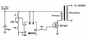
Voltage converter with stable 30V
The voltage converter (Fig. 12) allows you to obtain a stabilized voltage of 30 V at the output. A voltage of this magnitude is used to power varicaps, as well as vacuum fluorescent indicators.
Rice. 12. Circuit of a voltage converter with a stabilized output voltage of 30 V.
On a DA1 chip of type KR1006VI1, a master oscillator is assembled according to the usual circuit, producing rectangular pulses with a frequency of about 40 kHz.
A transistor switch VT1 is connected to the output of the generator, which switches the inductor L1. The amplitude of the pulses when switching the coil depends on the quality of its manufacture.
In any case, the voltage on it reaches tens of volts. The output voltage is rectified by diode VD1. A U-shaped RC filter and a zener diode VD2 are connected to the output of the rectifier. The voltage at the output of the stabilizer is entirely determined by the type of zener diode used. As a “high-voltage” zener diode, you can use a chain of zener diodes having a lower stabilization voltage.
Additional materials:
Articles:
- Maxim Integrated nanoPower Technology: When Low IQ Benefits
- Sleep Control: Improve Battery Efficiency with DC/DC MAX17225 nanoPower
- One choke for the entire system: Maxim multichannel converters with SIMO and nanoPower technologies
- Real-time power measurement using power logger IC
- Extending the runtime of portable electronics with a SIMO-based converter
- SIMO fighters: features of using Maxim SIMO converters
- Selecting a SIMO PMIC Converter for a Handheld Device Project
- Increasing the energy efficiency of portable devices using SIMO PMIC converters
News
- MAX17222 - long life for small things
- MAX38640/1/2/3 – step-down converters of the NanoPower family with ultra-low current consumption
- MAX17270 – NanoPower SIMO PMIC for IoT with ultra-low power consumption
•••
Concept of DC DC converters
As the name suggests, this type of device converts the DC input voltage into the same output voltage, but of a different rating. DC is an English abbreviation, Direct Current is direct current.
Since the presence of alternating voltage is fundamental for the operation of a transformer, a different principle is used in these converters. DC - DC devices come in two main types:
- Inverter systems, in which the DC voltage is first converted into an AC voltage of high frequency, which is supplied to a small-sized high-frequency transformer.
- Pulse ones, in which the main elements are a storage choke and a capacitor.
Strictly speaking, all of the listed devices belong to pulse devices, but these differences allow us to classify them into different groups.
External inspection, element base
Switching voltage stabilizer
Initially, dc dc converters were built on discrete analog elements. The circuits of such devices were highly complex and could only be done by trained specialists.
As the element base improved, in particular, with the advent of specialized integrated circuits, it became possible to create devices with a minimum number of parts, which also do not require configuration and adjustment.
Popular PWM controller chip
By complicating the elementary circuit from the technical documentation on the IC, you can significantly improve the performance of the converter. In particular, adding a powerful switching transistor increases the maximum load current, in contrast to directly switching on the IC.
Pulse width modulation
The output parameters are adjusted by controlling the duration of the open and closed states of the key element. The most common principle is pulse width modulation.
The transistor is switched by high-frequency pulses of constant frequency. Opening and closing times are determined by the width of the pulses. The tracking circuit monitors the output voltage by comparing it with a reference. The mismatch signal is sent to the modulator, which regulates the parameters of the control pulses.
Pulse width modulation
In modern designs, all these functions are assigned to a specialized integrated circuit, making the circuit design of switching power supplies with pulse width modulation (PWM) simple and reliable.