Single-phase bridge uncontrolled rectifier
The rectifier circuit (Fig. 17, a) includes a power transformer with one secondary winding and a rectifier bridge of four diodes VD1-VD4. Let us consider the principle of operation of the rectifier, taking the rectifier load to be purely active.
The output voltage ud with a purely active load has the form of unipolar half-waves of voltage u2 (Fig. 17, c). This is obtained as a result of alternately unlocking diodes VD1, VD2 and VD3, VD4.
Single phase bridge rectifier
Rice. 17. Single-phase bridge rectifier circuit (a)
and its timing diagrams (b-f)
Diodes VD1, VD2 are open in the interval at half-wave voltage u2 of positive polarity (shown in Fig. 17, a without brackets), created under the influence of voltage u1 (Fig. 17, b, c). Open diodes VD1, VD2 provide connection between the secondary winding of the transformer and the load, creating on it a voltage id of the same magnitude and polarity as the voltage u2 (Fig. 17, c). If there is a half-wave of voltage u1 of negative polarity in the interval, the polarity of voltage u2 is reversed. Under its influence, diodes VD3, VD4 are opened, connecting voltage u2 to the load with the same polarity as in the previous interval (Fig. 17, a, c). Due to the identity of the ud curves for the rectifiers (bridge and with transformer zero point output) for the circuit in Fig. 17, and relations (19), (20) between the rectified voltage Ud and the effective value of voltage U2 and relations (22)-(24) are valid, characterizing the harmonic composition and ripple factor of the output voltage. All parameters of the circuit are summarized in Table 3. Detailed calculations are given in [1, 2].
Since the current Id = Ud/RH (Fig. 17, d) is distributed equally between pairs of diodes (Fig. 17, d, e)
The reverse voltage is applied simultaneously to two non-conducting diodes within the conductivity range of the other two diodes. In this case, it is created by the voltage of the secondary winding of the transformer u2. The ub curve for diodes VD1 VD2 is shown in Fig. 17, f. The maximum reverse voltage is determined by the amplitude value of the voltage u2 (Table 3), i.e. it is half that in a circuit with a zero point output.
In the circuit under consideration, the parameters of the primary winding I1, U1 are related, respectively, to the parameters of the secondary winding I2, U2 by the transformation ratio n. In accordance with this, the calculated winding powers are the same and the transformer power ST = 1.23Pd (Table 3).
The advantages of a bridge rectifier circuit are a simpler transformer containing only one secondary winding, and a lower reverse voltage (for a given voltage Ud) for which diodes should be selected. These advantages compensate for the disadvantage of the circuit, which consists in a larger number of diodes. Therefore, the bridge circuit has found predominant application in single-phase rectifiers of low and medium power.
62. Single-phase zero controlled rectifier
The circuit of a single-phase controlled rectifier with a zero terminal, performed by analogy with the circuit of an uncontrolled rectifier (see Fig. 13, a), is shown in Fig. 23. We will analyze it for two types of load - purely active and active-inductive. Let us first assume that the load is purely active (key K1 is on, key K2 is off).
Single-phase zero controlled rectifier
The active load mode corresponds to the timing diagrams shown in Fig. 24, a-e. Let a positive half-wave of the network voltage u1 act at the input of the rectifier (Fig. 24, a), which corresponds to the polarity of the voltages on the transformer windings indicated in Fig. 23 without parentheses. During the interval, thyristors T1, T2 are closed, the voltage at the rectifier output is ud=0 (Fig. 24, c). The total voltage of the two secondary windings of the transformer u2-1+u2-2 is applied to thyristors T1, T2. The voltage acts on thyristor T1 in the forward direction, and on thyristor T2 - in the reverse direction. If the resistances of non-conducting thyristors at forward and reverse voltages are considered the same, then during the interval the voltage on the thyristors (taking into account the corresponding polarity) will be determined by the value (u2-1—u2-2)/2 = u 2 (Fig. 24, e).
At the moment of time determined by the angle , a pulse is received from the control system of the rectifier control system to the control electrode of thyristor T1 (Fig. 24, b). As a result of unlocking, thyristor T1 connects the load Rн to the voltage u2-1=u2 of the secondary winding of the transformer. At the load in the interval, voltage ud is formed (Fig. 24, c), which is a section of the voltage curve u2-1=u2. Current flows through the load and thyristor T1 (Fig. 24, d) id = ial = ud/Rн. When the supply voltage passes through zero ( ), the current of thyristor T1 becomes equal to zero and the thyristor closes.
During the interval, the polarity of the supply voltage is reversed. During this interval, both rectifier thyristors are closed. A reverse voltage is applied to thyristor T1 (Fig. 24, e), and a forward voltage equal to T2 is applied to thyristor T2.
Timing diagrams
Timing diagrams illustrating the principle of operation of a single-phase controlled rectifier with a zero terminal under a purely resistive load.
At the end of the specified interval, an unlocking pulse is sent to thyristor T2. Unlocking this thyristor causes the application of a voltage ud=u2-2=u2 (Fig. 24, c) to the load of the same shape as in the conduction interval of thyristor T1. The current id = ia2 = ud/Rн flows through the load and the thyristor (Fig. 24, d). During the conduction interval of thyristor T2, the voltages of the two secondary windings of the transformer are connected to thyristor T2, as a result of which, from the moment thyristor T2 is unlocked, a reverse voltage equal to 2u2 acts on thyristor T1 (Fig. 6.2, e). The maximum reverse voltage corresponds to the value Ubmax=2 U2, where U2 is the effective value of the secondary voltage of the transformer. Subsequently, the processes in the circuit follow similar to those discussed. The currents of the secondary windings of the transformer are determined by the currents of thyristors T1, T2 (Fig. 24, d, e). The primary current i1 (Fig. 24, a) is connected to the secondary currents by the transformation ratio of the transformer and has pauses at intervals. Its first harmonic has a phase shift towards the lag relative to the supply voltage.
A feature of a controlled rectifier is its ability to regulate the average value of the rectified voltage Ud when the angle changes (Fig. 24, c). At = 0, the output voltage curve ud corresponds to the case of an uncontrolled rectifier (see §7) and the voltage is maximum. The control angle (180 el. degrees) corresponds to ud = 0 and Ud = 0. In other words, the controlled rectifier when the angle changes from 0 to 180 el. the hail regulates the voltage Ud ranging from a maximum value of 0.9U2 to zero. The appearance of the ud curves at different angle values is shown in Fig. 25, a-g.
The dependence of the voltage Ud on the angle is called the control characteristic of the controlled rectifier. It is determined from the expression for the average voltage across the load. This voltage in the interval corresponds to the secondary voltage sinusoid (see Fig. 24, c or 25, b, c), i.e.
.
The calculation result gives
,
where Ud0 = 0.9U2 is the average voltage across the load at .
Output voltage curves of a single-phase rectifier at
pure resistive load and different control angles
Regulating characteristic
single-phase controlled rectifier
63. Three-phase zero controlled rectifier
The peculiarity of the operation of a three-phase zero-controlled rectifier is the delay by the angle of the unlocking moment of the next thyristors relative to the natural unlocking points having coordinates, etc. (Fig. 31, b).
Three-phase zero controlled rectifier
Diagram of a three-phase zero controlled rectifier (a), its timing diagrams (b) and adjustment characteristic (c)
In the rectified voltage curve, sections of the sinusoid are cut out, as a result of which the average voltage value Ud decreases. Thus, when the angle changes, the value of Ud is adjusted.
The effect of changing the angle on the ud curve and the average voltage Ud are shown in Fig. 31, b. The ud curve in Fig. 31, b, consists of sections of phase voltages of the secondary windings of the transformer ua, ub, uc.
When the angle changes in the range from 0 to 30° (Fig. 31, b), the transition of voltage ud from one phase voltage to another occurs within the positive polarity of the phase voltage sections. Therefore, the shape of the voltage curve ud and its average value are the same for both active and active-inductive loads. The load current is continuous.
At >30°, the shape of the ud curve depends on the nature of the load (Fig. 31, b). The reason for the dependence is the same as in controlled single-phase rectifiers (see §12). In the case of an active-inductive load, current id continues to flow through the thyristors and secondary windings of the transformer after changing the polarity of their phase voltage, and therefore sections of phase voltages of negative polarity appear in the curve. When these sections continue until the next moment the thyristors are unlocked. The equality of the areas of the plots and the condition Ud=0 corresponds to the angle =90°. The value of this angle characterizes the lower limit of voltage regulation Ud at . With an active load, there are no voltage sections of negative polarity and zero pauses appear in the ud curve at > 30°. The voltage Ud=0 will now correspond to the angle = 150o.
The dependence of the average value of the rectified voltage on the angle (regulating characteristic) at can be found by averaging the curve ud over an interval of 2:
,
i.e., it is determined by the same relationship as in single-phase circuits.
The section of the adjustment characteristic under active load ( ) in the interval 150° > > 30° is found from the expression
.
In this case, the closing of the thyristor occurs at the point corresponding to zero voltage earlier than the opening of the next thyristor. Thyristor conductivity interval from to π. The load current is interrupted.
The control characteristics of a three-phase bridge rectifier, constructed using expressions (59), (60), are shown in Fig. 31, v. The ambiguity of the control characteristics and the intermittent current zone can be eliminated by shunting the load with a freewheeling diode. The control characteristic in this case will be similar to the characteristic of operation on an active load, and the zone of intermittent current in the load in the limit will be narrowed to zero due to the closure of the current in the circuit, the content of the emf. loads and freewheeling diode.
Single-phase rectifier with zero tap
SECONDARY POWER SUPPLY SOURCES
ELECTRONIC DEVICES
Block diagram of secondary power supplies
Secondary power sources are devices designed to convert the energy of a primary power source, which, in particular, is an alternating current network, into electrical energy to supply various types of consumers of this energy. One of these energy consumers is electronic equipment, which, as a rule, requires a highly stable DC voltage with a certain nominal value. For example, electronic equipment using integrated circuits requires a low-level constant voltage (± 5 - ± 15 V) with stability (± 5 - 10)% for its power supply. Secondary power supplies for electronic equipment are built using electronic devices.
Figure 6.1. Block diagram and timing diagrams
voltage of secondary power supplies
at the input and output of its nodes
The block diagram of a typical secondary power supply for electronic equipment is shown in Fig. 6.1. It includes a network transformer (T), a rectifier (V), a ripple filter (F) and an output voltage stabilizer (SN). The same figure shows the sequence of mains voltage conversion. The stabilizer not only changes the network voltage to the required level, but also galvanically isolates the load from the power network. The rectifier, which is the main component of the secondary power source, ensures the unidirectional flow of current, characterized by a certain level of ripple. As a valve, it uses electronic devices that have the property of one-way conductivity. The filter reduces voltage ripples at the rectifier output. For this purpose, low-pass filters based on passive and sometimes active elements are used. The voltage stabilizer is designed to eliminate the influence of external influences on the output voltage of the secondary power supply, which include changes in the network voltage and load parameters. Secondary power supplies may also include various auxiliary elements and components intended for control, automation and protection.
Depending on the type of primary power supply, there are single-phase and three-phase rectifiers. Rectifiers, which are called controlled, can also regulate the rectified voltage. The circuits of single-phase uncontrolled rectifiers are discussed below.
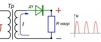
Single-phase rectifier with zero tap
The diagram of a single-phase rectifier with a zero tap from the secondary winding of the transformer is shown in Fig. 6.2. It consists of a power transformer with a split secondary winding, which consists of two identical halves. Voltages are removed from each half of this winding, identical in magnitude, but shifted in phase by 180° relative to the zero point, as well as two diodes D1 and D2.
Figure 6.2. Single-phase rectifier circuit with zero tap
The operating principle of the rectifier is considered for the case of active load RH. In this case, time diagrams of voltages and currents are used, which are shown in Fig. 6.3. Figures 6.3,a and 6.3,b show the time dependences of the voltage u1 supplied from the network, supplied to the primary winding of the transformer, and the voltages u2-1 and u2-2, removed from each half of the secondary winding. To get a complete picture of the operation of the rectifier, it is enough to consider the processes occurring in the rectifier in the phase range from 0 to , i.e. during one period of applied voltage.
Figure 6.3. Timing diagrams illustrating operation
single-phase rectifier with zero tap
In the phase interval 0÷, when there is a positive half-cycle of voltage at the input of the transformer, a positive voltage is applied to the anode of diode D1, and a negative voltage is applied to the anode of diode D2. Therefore, diode D1 is in the open state, and diode D2 is in the closed state. The current under such conditions flows through the upper half of the secondary winding of the transformer, diode D1 and load RN. A voltage is created in the load, the time dependence of which, if the voltage drop in the open diode is neglected, coincides with the time dependence of the voltage u2-1, which is illustrated by the “positive half-wave” in Fig. 6.3c. The voltage amplitudes are the same.
In the phase interval ÷, a negative half-cycle of voltage acts at the input of the transformer, and diode D 2 is in the open state, and diode D 1 is in the closed state. Current flows through the lower half of the secondary winding of the transformer, diode D 2 and the load. In this case, the direction of the current in the load will be the same as in the phase interval 0y. Consequently, in the phase interval ÷, the voltage in the load also has a positive polarity. In Fig. 6.3c, where the time dependence of the voltage at the output of the rectifier is shown, the numbers of diodes through which current flows during certain half-cycles of the supply voltage are indicated.
The current flowing through the load is determined by Ohm's law
. (6.1)
It has the same time dependence as voltage (Fig. 6.3d).
As can be seen from Fig. 6.3, c and 6.3, d, the voltage and current at the output of the rectifier are in the form of pulses of positive polarity. The expansion of periodic functions into a Fourier series allows us to isolate the constant and variable components of voltage and current. For the rectified voltage consumer, the constant component is important, which can be defined as the average voltage value.
Since the period of the rectified voltage corresponds to a phase interval of width , within which the voltage changes as a function of sine, for its constant component we can write:
, (6.2)
where is the effective value of the voltage removed from one of the halves of the secondary winding of the transformer. A similar relationship can be written for the direct component of the rectified current:
. (6.3)
Load current amplitude
. (6.4)
The values of the constant components of rectified voltage and current in Fig. 6.3,c and 6.3,d are represented by horizontal solid straight lines.
The diodes are in the open and closed states alternately, and current flows through each diode during one half-cycle of the supply voltage, as shown in Fig. 6.3, e, f. Therefore, the average diode current is half the average load current.
. (6.5)
The amplitude values of the currents in the diodes and the load are the same.
When the diode is closed, a negative voltage is applied to it, the value of which varies according to a sinusoidal law, as shown in Fig. 6.3g for diode D1. The amplitude of this voltage is equal to twice the amplitude of the voltage removed from one of the halves of the secondary winding of the transformer, since voltage is supplied to the closed diode from the two extreme taps of this winding. Therefore, the maximum amount of reverse voltage that a diode must withstand is
. (6.6)
Relations (6.5) and (6.6) are used when choosing the type of diode that is supposed to be used in the rectifier.
The quality of the rectified voltage is assessed by a parameter called ripple factor, which is defined as the ratio of the amplitude of the th harmonic of the rectified voltage to the value of the constant voltage component. The magnitudes of the amplitudes of the harmonic components of voltage are determined by the Fourier series expansion of the function
The first harmonic has the largest amplitude, for which the ripple coefficient is
(6.8)
At mains frequency = 50 Hz, the frequency of the first harmonic at the rectifier output is 100 Hz.
Models of uncontrolled and controlled rectifiers
The operation of the controlled rectifier shown in Fig. 3.10 comes down to a cyclic change of two types of circuit states:
1). Conduction state when two thyristors are open ( VSA
(
a
) anode (
a
) group of phase
A
and thyristor
VSB
(
k
) cathode (
k
) group of phase
B
) and the load is under linear voltage
eAB
(Fig. 3.11,a);
2). Switching state when three thyristors are open ( VSA
(
a
) anode (
a
) group of phase
A
, thyristor
VSB
(
k
) cathode (
k
) group of phase
B
and thyristor
VSC
(
k
) cathode (
k
) group of phase
C
) and current switching occurs in two thyristors (Fig. 3.11,b
VSC
(
k
put into operation
VSB
(
k
output .
Figure 3.10 — Controlled rectifier circuit
In Fig. 3.11, open thyristors are shown with jumpers marked with load current iH
, switching current
iK
VSC
(
k
being put into operation and switching current
iδ
VSB
(
k
being taken out of operation .
Figure 3.11 — States of the three-phase bridge controlled rectifier circuit
The switching circuit (Fig. 3.11b) is described by a system of equations:
or
(3.21)
The circuit in the conduction state (Fig. 3.11a) is described by a system of equations
(3.22)
Combining expressions (3.21) and (3.22) for two states of the circuit gives
(3.23)
where F1
and
F7
are functions of the state of the circuit (switches), taking values
0
or
1
, and the function
F1
determines the conduction interval (with
F1=1
), and the function
F7
determines the switching interval (with
F7=1
).
A generalization of expression (3.23) to all possible states of the circuit in Fig. 3.10 is
(3.24)
where eH=
(
F1-F4
)
eAB+
(
F3-F6
)
eBC+
(
F5-F2
)
eCA
– generalized emf applied to the load;
eK=
(
F1-F4
)
eBC+
(
F3-F6
)
eCA+
(
F5-F2
)
eAB
– generalized emf acting in the commutation circuit.
When modeling, it is convenient instead of the argument - time t
use a phase variable
θ
, which is related to time by the dependence
θ=ωt
.
Then in system (3.24) inductance L
will be replaced by inductive reactance
X
in accordance with the relation
X=ωt
. System (3.24) will take the form
(3.25)
Graphs of state functions F1…F7
are shown in Fig. 3.12.
Functions F1...F6
set the conductivity intervals of the circuit in its different states, and function
F7
sets the switching intervals.
In Fig. 3.12 it is indicated: α
is the rectifier control angle,
λ
is the conduction angle during the circuit operation cycle,
γ
is the thyristor switching angle.
The end of thyristor switching is determined by the moment in time when the current iδ
goes to zero.
F
is nonzero .
The model of an uncontrolled rectifier is a special case of a controlled one, when the control angle α
equals
0
.
Figure 3.12 — Functions of the state of the circuit, values of ен and ек at conductivity intervals and values of angles α, γ and λ
Questions for self-control
1. What are the states of a controlled rectifier circuit?
2. Give a system of equations for the switching state of a controlled rectifier circuit.
3. Give a system of equations for the conductivity state of a controlled rectifier circuit.
4. How is the value of the generalized emf applied to the load determined?
5. How is the value of the generalized emf applied to the commutation circuit determined?
6. Explain the procedure for replacing the time argument t with the angle argument θ in the model.
7. Explain the graphs shown in Fig. 3.12.
Literature [1-9]
3.8 Methodology for modeling converter equipment devices
The operation of converter technology devices is reduced to a cyclic change of a finite number of circuit states. Since the individual states of the circuit are similar to each other, a generalized description of the circuit by one system of equations is possible, into which variable state functions (keys) are introduced. Then the enumeration of all states of the circuit is reduced to enumeration of the values of state functions, and not of circuits and systems of equations, which, of course, significantly simplifies the modeling.
The values of the state functions depend on the tick number during the repetition period of the circuit. It is advisable to introduce a clock number function, the value of which, according to the above graphs of state functions, can determine the values of these functions. Figure 3.13 shows such a program and the result of its execution. The program uses the floor
(
X
) definition of the integer part of the
number
X. In the above program, calculations are carried out using the variable t
, which can easily be converted into calculations using the variable
θ
.
Figure 3.13 — Program for calculating function n
(
t
) number of measures in the period
repeatability of converter device states
Next, a generalized system of equations is solved with the values of the state functions determined in the process of calculation. Methods for calculating state functions depending on t
or from
θ
for different types of converter devices have both much in common and also have features due to the specifics of the circuits and algorithms of their operation.
Simulation of an autonomous voltage inverter
(
Fig.3.7
)
Let us rewrite the system of equations (3.19) in matrix form
(3.26)
Solution of system (3.29) with respect to variables piA, piB, piC
is a matrix
S
(
t,i
) of size
3x1
, which is determined in the MathCAD package using the standard
lsolve
for solving a system of linear equations:
S
(
t,i
)
:=lsolve
(
M
(
t),N
(
t,i
)) (3.27)
Solution S
(
t,i
) has Cauchy normal form and can therefore be used in the standard
Rkadapt
for solving a system of differential equations:
z:=Rkadapt
(
iSTART, tSTART, tSTOP, NOUT, S
(
t,i
)), (3.28)
where iSTART
— vector of initial conditions for currents
iA
,
iB
and
iC
.
The values of the state functions can be determined in accordance with Table 3.1 and Fig. 3.13 expressions
(3.29)
From these expressions the values of the switching functions are determined as
F1
(
t
)
=F
(
t
)
0, F2
(
t
)
=F
(
t
)
1, F3
(
t
)
=F
(
t
)
2,
F4
(
t
)
=F'
(
t
)
0, F5
(
t
)
=F'
(
t
)
1, F6
(
t
)
=F'
(
t
)
2
(3.30)
If we take into account the equalities arising from Table 3.1
F1
(
t
)
+F2
(
t
)
+F3
(
t
)
=0, F4
(
t
)
+F5
(
t
)
+F6
(
t
)
=0
(3.31)
then expressions (3.29) can be simplified - instead of calculating matrices from three lines, it is enough to calculate matrices from two lines, for example F1
(
t
)
, F2
(
t
) and
F4
(
t
)
, F5
(
t
).
Simulation of a controlled rectifier
(
Fig.3.10
)
The output to the function for solving differential equations of the form (3.28) is the same as when modeling the AIN.
The argument of all functional dependencies is the variable θ
with an arbitrary range of change.
From it a variable φ
(
θ
) is formed with a range of changes equal to
2π
:
(3.32)
Linear voltages will be calculated using the formulas
(3.33)
Since the graphs of state functions for a rectifier (Fig. 3.12) are significantly different from the graphs for AIN (Fig. 3.8), the method of determining them for a rectifier will be significantly different than for AIN, given by expressions (3.29), (3.30) and ( 3.31).
The following calculations are performed:
1). The row matrix F0:=|0 0 0 0 0 0 0
|, which by transposing
F:=F0T
turns into a columnar matrix
F
.
2). Index n1
(
θ
) active line voltage in the thyristor switching phase
(3.34)
3). The moment of formation of the opening pulse to the thyristor and at the same time the beginning of the thyristor switching process is determined
(3.35)
In order for the equality to be satisfied, it is necessary to set the value α
multiple of the step of changing the angle
θ
.
4). The moment of completion of switching of thyristors and the transition to the conduction state of the circuit is determined
(3.36)
Questions for self-control
1. How is size n determined
(
t
)
clock state of the circuit as a function of current time t?
2. How is the system of differential equations of the AIN model reduced to normal form?
3. Create formulas to determine the values of the state function F1, F2 and F3 of the AIN model depending on the cycle number n
(
t
).
4. Create formulas to determine the values of the state function F4, F5 and F6 of the AIN model depending on the cycle number n
(
t
).
5. Give the formula for converting the angle θ, which varies in an arbitrary range, to the angle φ
(
θ
)
with a range from 0 to 2π.
6. Explain the calculation algorithm used in modeling rectifiers.
Literature [1-9]