Just twenty-five years ago, radio amateurs and older generation specialists had to study new devices at that time - transistors. It was not easy to give up the vacuum tubes that we were so accustomed to and switch to the crowding and ever-expanding “family” of semiconductor devices.
And now this “family” has increasingly begun to give way in radio engineering and electronics to the latest generation of semiconductor devices - integrated circuits, often called ICs for short.
What is an integrated circuit
An integrated circuit is a miniature electronic unit containing in a common housing transistors, diodes, resistors and other active and passive elements, the number of which can reach several tens of thousands.
One microcircuit can replace an entire unit of a radio receiver, an electronic computer (computer) and an electronic machine. The “mechanism” of a digital wristwatch, for example, is just one larger chip.
According to their functional purpose, integrated circuits are divided into two main groups: analog, or linear-pulse, and logical, or digital, microcircuits.
Analog microcircuits are intended for amplification, generation and conversion of electrical oscillations of different frequencies, for example, for receivers, amplifiers, and logical ones - for use in automation devices, in devices with digital timekeeping, in computers.
This workshop is devoted to familiarization with the device, operating principle and possible application of the simplest analog and logical integrated circuits.
DIP package
DIP ( Dual I n-Line Package ) - a package with two rows of pins on the long sides of the microcircuit . Previously, and probably still now, the DIP package was the most popular package for multi-pin microcircuits. It looks like this:
Depending on the number of pins of the microcircuit, after the word “DIP” the number of its pins is placed. For example, a microcircuit, or more precisely, an atmega8 microcontroller, has 28 pins:
Therefore, its housing will be called DIP28.
But this microcircuit’s housing will be called DIP16.
In order not to count the number of pins each time, you can count them only on one side of the microcircuit and stupidly multiply them by two.
Basically, logic chips, operational amplifiers, etc. were produced in the DIP package in the Soviet Union. Nowadays, the DIP package also does not lose its relevance and various microcircuits are still made in it, ranging from simple analog ones to microcontrollers.
The DIP housing can be made of plastic (which is in most cases) and is called PDIP , as well as ceramic - CDIP . The CDIP's body feels rock-hard to the touch, which isn't surprising since it's made of ceramic.
Example of CDIP enclosure.
There are also modifications of the DIP housing: HDIP, SDIP.
HDIP ( H eat-dissipating DIP ) - heat dissipating DIP. Such microcircuits pass a large current through themselves, so they become very hot. To remove excess heat, such a microcircuit must have a radiator or something similar, for example, like here are two radiator wings in the middle of the microchip:
SDIP ( S mall DIP ) - small DIP. The microcircuit is in a DIP package, but with a small distance between the legs of the microcircuit:
On an analog chip
Of the huge “family” of analogue ones, the simplest are the twin microcircuits K118UN1A (K1US181A) and K118UN1B (K1US181B), which are part of the K118 series.
Each of them is an amplifier containing... However, it’s better to talk about the electronic “stuffing” later. For now, we will consider them “black boxes” with pins for connecting power supplies, additional parts, input and output circuits to them.
The difference between them lies only in their amplification factors for low-frequency oscillations: the gain factor of the K118UN1A microcircuit at a frequency of 12 kHz is 250, and the K118UN1B microcircuit is 400.
Rice. 1. Microcircuit and circuit based on it.
At high frequencies, the gain of these microcircuits is the same - approximately 50. So, any of them can be used to amplify oscillations of both low and high frequencies, and therefore for our experiments. The appearance and symbols of these amplifier microcircuits on the circuit diagrams of the devices are shown in Fig. 1.
They have a rectangular plastic body. On the top of the case there is a mark that serves as a reference point for the pin numbers. The microcircuits are designed for power from a DC source with a voltage of 6.3 V, which is supplied through pins 7 (+Upit) and 14 (- Upit).
The power source can be an AC power supply with adjustable output voltage or a battery made up of four cells 334 and 343.
The first experiment with the K118UN1A (or K118UN1B) microcircuit was carried out according to the diagram shown in Fig. 89. As a mounting board, use a cardboard plate measuring approximately 50X40 mm.
Solder the microcircuit with pins 1, 7, 8 and 14 to wire brackets passed through punctures in the cardboard. All of them will serve as racks holding the microcircuit on the board, and the brackets of pins 7. and 14, in addition, will serve as connecting contacts with the GB1 battery (or the mains power supply).
Between them, on both sides of the microcircuit, strengthen two or three more contacts, which will be intermediate for additional parts. Mount capacitors C1 (type K50-6 or K50-3) and C2 (KYAS, BM, MBM) on the board, connect headphones B2 to the output of the microcircuit.
Connect (via capacitor C1) an electrodynamic microphone B1 of any type or a DEM-4m telephone capsule to the input of the microcircuit, turn on the power and, pressing the phones more tightly to your ears, tap lightly on the microphone with a pencil. If there are no errors in the installation, sounds resembling clicks on a drum should be heard in the phones.
Ask a friend to say something in front of the microphone - you will hear his voice on the phones. Instead of a microphone, you can connect a radio broadcast (subscriber) loudspeaker with its matching transformer to the input of the microcircuit. The effect will be about the same.
Continuing the experiment with a single-acting telephone device, connect between the common (negative) conductor of the power circuit and pin 12 of the microcircuit the electrolytic capacitor C3, indicated in the diagram by dashed lines. At the same time, the sound volume on phones should increase.
Telephones will sound even louder if the same capacitor is connected to pin 5 (in Fig. 1 - capacitor C4). But if the amplifier is excited, then between the common wire and pin 11 you will have to connect an electrolytic capacitor with a capacity of 5 - 10 µF. nominal voltage 10 V.
Another experiment: connect a ceramic or paper capacitor with a capacity of 5 - 10 thousand picofarads between pins 10 and 3 of the microcircuit. What happened? An incessant medium-pitched sound appeared on phones. As the capacitance of this capacitor increases, the sound tone in telephones should decrease, and with decrease, it should increase. Check this.
Rice. 2. Internal circuit of the microcircuit.
Now let’s open this “black box” and look at its “filling” (Fig. 2). Yes, this is a two-stage amplifier with direct coupling between its transistors. Silicon transistors, n-p-n structures. The low-frequency signal generated by the microphone is supplied (via capacitor C1) to the input of the microcircuit (pin 3).
The voltage drop created across resistor R6 in the emitter circuit of transistor V2 is supplied through resistors R4 and R5 to the base of transistor VI and opens it. Resistor R1 is the load of this transistor. The amplified signal taken from it goes to the base of transistor V2 for additional amplification.
In the experimental amplifier, the load of transistor V2 was headphones included in its collector circuit, which converted the low-frequency signal into sound.
But its load could be resistor R5 of the microcircuit if pins 10 and 9 are connected together. In this case, the telephones must be connected between the common wire and the connection point of these pins through an electrolytic capacitor with a capacity of several microfarads (the positive plate to the microcircuit).
When the capacitor was connected between the common wire and pin 12 of the microcircuit, the sound volume increased. Why? Because, by shunting resistor R6 of the microcircuit, he weakened the negative alternating current feedback operating in it.
The negative feedback became even weaker when you connected the second capacitor to the base circuit of transistor V1. And the third capacitor, connected between the common wire and pin 11, formed an decoupling filter with resistor R7 of the microcircuit, preventing excitation of the amplifier.
What happened when you connected a capacitor between pins 10 and 5? He created a positive feedback between the output and input of the amplifier, which turned it into an audio frequency oscillator.
So, as you can see, the K118UN1B (or K118UN1A) microcircuit is an amplifier that can be low-frequency or high-frequency, for example, in a receiver. But it can also become a generator of electrical oscillations of both low and high frequencies.
Brief historical background
The first experiments in creating semiconductor integrated circuits were carried out in 1953, and industrial production of integrated circuits began in 1959. In 1966, production of integrated circuits of medium degree of integration began (the number of elements in one crystal is up to 1000). In 1969, integrated circuits with a higher degree of integration (large-scale integrated circuits, LSI) were created, containing up to 10,000 elements in one chip.
In 1971, microprocessors were developed, and in 1975, very-large-scale integrated circuits (VLSI), containing more than 10,000 elements in a single chip. It is useful to note that the limiting frequency of bipolar transistors in semiconductor integrated circuits reaches 15 GHz or more.
By 2000, integrated circuits are expected to appear containing up to 100 million MOS transistors in a single chip (we are talking about digital circuits). Notation system. The symbol for integrated circuits includes the main classification features.
- The first element is a number corresponding to the design and technological group. The numbers 1, 5, 6 and 7 in the first element indicate semiconductor integrated circuits. Hybrid chips are assigned the numbers 2, 4 and 8. Film, vacuum and ceramic integrated circuits are designated by the number 3.
- The second element, which determines the serial development number of the series, consists of two (00 to 99) or three (000 to 999) digits.
- The third element, indicating the subgroup and type of microcircuit, consists of two letters.
- The fourth element, indicating the serial number of the development of the microcircuit of this series, consists of one or more digits.
It will be interesting➡ Making a laboratory power supply with your own hands
Other classification features can be added to these basic elements of microcircuit designations.
Structure of an integrated circuit
An additional letter at the beginning of the four-element designation indicates a design feature:
- P - plastic housing type DIP;
- A - plastic planar body;
- E - metal-polymer housing of the DIP type;
- C - glass-ceramic body of DIP type;
- I - glass-ceramic planar body;
- N - ceramic “leadless” housing.
At the beginning of the designation for microcircuits used in widespread use, the letter K is given.
Series of unpackaged semiconductor microcircuits begin with the number 7, and unpackaged analogues of packaged microcircuits are designated by the letter B before the series indication.
A hyphen after the designation indicates a number characterizing the modification of the design:
- 1 - with flexible leads;
- 2 - with strip (spider) leads, including those on a polyamide carrier;
- 3 - with rigid leads;
- 4 - on a common plate (undivided);
- 5 - separated without loss of orientation (pasted on film);
- 6 - with contact pads without leads.
How are integrated circuits created?
How to make a memory chip or computer processor? The manufacturing process begins with the chemical element silicon, which is chemically treated (alloyed) to impart different electrical properties.
A modern design of an integrated circuit (one of many forms) installed on the electronic board of the device. This is far from the most advanced option, but only one of many
Traditionally, materials of two categories are used for electronics needs:
- Conductors.
- Insulators.
But technically, everything is more complicated, especially when it comes to certain elements in the middle of the periodic table (groups 14 and 15), in particular silicon and germanium. What is noteworthy is that insulating materials can become conductors if a certain amount of impurities is added to these materials. A process known as alloying.
The principle of alloying chemical elements
If you add some antimony to silicon, the structure of this chemical element is saturated with more electrons than usual. Conducts electricity. Silicon "doped" in this way takes on the N-type characteristic. In another case, when boron is added instead of antimony, the mass of silicon electrons decreases, leaving peculiar “holes” that function like “negatively charged electrons.”
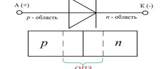
The holes allow positive electrical current to flow in the opposite direction. This type of silicon is characterized by P-type. Placing N-type and P-type silicon regions next to each other creates a junction that exhibits electron behavior characteristic of semiconductor-based electronic components:
- diodes,
- transistors,
- storage devices and others.
Enlarged photo of integrated circuits
Microcircuit in a radio receiver
We propose to test this microcircuit in the high-frequency path of a receiver assembled, for example, according to the circuit shown in Fig. 3. The input circuit of the magnetic antenna of such a receiver is formed by coil L1 and variable capacitor C1. The high-frequency signal of the radio station to which the circuit is tuned is sent through the coupling coil L2 and the separating capacitor C2 to the input (pin 3) of the L1 microcircuit.
From the output of the microcircuit (pin 10, connected to pin 9), the amplified signal is fed through capacitor C4 to the detector, diodes VI and V2 of which are connected according to the voltage multiplication circuit, and the low-frequency signal allocated to it is converted into sound by phones B1. The receiver is powered by a GB1 battery, composed of four 332, 316 cells or five D-01 batteries.
Rice. 3. Receiver circuit on a microcircuit.
In many transistor receivers, the high-frequency amplifier is formed by transistors, but in this one it is a microcircuit. This is the only difference between them.
Having the experience of previous workshops, I hope you will be able to independently mount and set up such a receiver and even, if you wish, supplement it with a low-frequency amplifier for loud-speaking radio reception.
SOIC package
The largest representative of this class of microcircuits are microcircuits in the SOIC ( S mall - Outline I ntegrated C circuit) - a small microcircuit with pins on the long sides. It is very similar to DIP, but pay attention to its conclusions. They are parallel to the surface of the body itself:
This is how they are soldered on the board:
Well, as usual, the number after “SOIC” indicates the number of pins of this microcircuit. The photo above shows microcircuits in the SOIC16 package.
On a logic chip
An integral part of many digital integrated circuits is the AND-NOT logical element, the symbol of which you see in Fig. 4, a. Its symbol is the "&" sign placed inside a rectangle, usually in the upper left corner, replacing the conjunction "AND" in English. There are two or more inputs on the left, one output on the right.
The small circle that begins the communication line of the output signal symbolizes the logical Negation “NOT” at the output of the microcircuit. In the language of digital technology, “NOT” means that the NAND element is an inverter, that is, a device whose output parameters are opposite to the input ones.
The electrical state and operation of a logic element are characterized by the signal levels at its inputs and output. A small (or zero) voltage signal, the level of which does not exceed 0.3 - 0.4 V, is usually called (in accordance with the binary number system) logical zero (0), and a higher voltage signal (compared to logical 0), the level of which can be 2.5 - 3.5 V, - logical unit (1).
For example, they say: “the output of the element is logical 1.” This means that at the moment a signal has appeared at the output of the element, the voltage of which corresponds to the logical level 1.
In order not to delve into the technology and structure of the NAND element, we will consider it as a “black box”, which has two inputs and one output for an electrical signal.
The logic of the element is that when logical O is applied to one of its inputs, and logical 1 is applied to the second input, a logical 1 signal appears at the output, which disappears when signals corresponding to logical 1 are applied to both inputs.
For experiments that memorize this property of the element, you will need the most common K155LAZ microcircuit, a DC voltmeter, a fresh 3336L battery and two resistors with a resistance of 1...1.2 kOhm.
Rice. 4. Logical elements of the K155LAZ microcircuit.
The K155LAZ microcircuit consists of four 2I-NOT elements (Fig. 4, b), powered by one common DC source of 5 V, but each of them operates as an independent logical device. The number 2 in the name of the microcircuit indicates that its elements have two inputs.
In appearance and design, it, like all microcircuits of the K155 series, does not differ from the already familiar analog microcircuit K118UN1, only the polarity of connecting the power source is different. Therefore, the cardboard board you made earlier is suitable for experiments with this microcircuit. The power source is connected: +5 V - to pin 7" - 5 V - to pin 14.
But these conclusions are not usually indicated on a schematic diagram of the microcircuit. This is explained by the fact that on circuit diagrams the elements that make up the microcircuit are depicted separately, for example, as in Fig. 4, c. For experiments, you can use any of its four elements.
Solder the microcircuit with pins 1, 7, 8 and 14 to the wire stands on the cardboard board (as in Fig. 1). One of the input pins of any of its elements, for example, an element with pins 1 - 3, is connected through a resistor with a resistance of 1...1.2 kOhm to pin 14, the pin of the second input is directly connected to the common (“grounded”) conductor of the power circuit, and Connect a DC voltmeter to the output of the element (Fig. 5, a).
Turn on the power. What does the voltmeter show? A voltage of approximately 3 V. This voltage corresponds to a logic 1 signal at the output of the element. Using the same voltmeter, measure the voltage at the output of the first input. And here, as you can see, it is also logical 1. Therefore, when one of the inputs of the element is logical 1, and the second is logical 0, the output will be logical 1.
Rice. 5. Voltage measurements on a logic element.
Now connect the output of the second input through a resistor with a resistance of 1...1.2 kOhm to terminal 14 and at the same time with a wire jumper - with a common conductor, as shown in Fig. 5 B.
In this case, the output, as in the first experiment, will be logical 1. Next, watching the voltmeter needle, remove the jumper wire so that a signal corresponding to logical 1 is sent to the second input.
What does a voltmeter record? The signal at the output of the element is converted to logical 0. This is how it should be! And if any of the inputs are periodically shorted to a common wire and thereby simulate the supply of a logical 0 to it, then current pulses will appear at the output of the element with the same frequency, as evidenced by fluctuations in the voltmeter needle. Check this out experimentally.
The property of the NAND element to change its state under the influence of input control signals is widely used in various digital computing devices. Radio amateurs, especially beginners, very often use a logic element as an inverter - a device whose output signal is opposite to the input signal.
The following experiment can confirm this property of the element. Connect the terminals of both inputs of the element together and, through a resistor with a resistance of 1...1.2 kOhm, connect them to pin 14 (Fig. 5, c).
This way you will apply a signal corresponding to logical 1 to the common input of the element, the voltage of which can be measured with a voltmeter. What is the output?
The voltmeter needle connected to it slightly deviated from the zero scale mark. Here, therefore, as expected, the signal corresponds to logical 0.
Then, without disconnecting the resistor from pin 14 of the microcircuit, connect the input of the element to the common conductor with a wire jumper several times in a row (shown in Fig. 5, c by a dashed line with arrows) and at the same time watch the voltmeter arrow.
So you will be convinced that when the inverter input is logical 0, the output is logical 1 and, conversely, when the input is logical 1, the output is logical 0.
This is how an inverter works, especially often used by radio amateurs in the pulse devices they construct.
Rice. 6. Circuit diagram of an AF signal generator on a microcircuit.
An example of such a device is a pulse generator assembled according to the circuit shown in Fig. 6. You can verify its functionality right away, spending just a few minutes on it.
The output of element D1.1 is connected to the inputs of element D1.2 of the same microcircuit, its output is connected to the inputs of element DJ.3, and the output of this element (output ) is connected to the input of element D1.1 through a variable resistor R1. To the output of element D1.3 (between pin 8 and the common conductor) connect headphones B1, and electrolytic capacitor C1 in parallel with elements D1.1 and D1.2.
Set the variable resistor motor to the right (according to the diagram) position and turn on the power - you will hear a sound in the phones, the tone of which can be changed with a variable resistor.
In this experiment, elements D1.1, D1.2 and D1.3, connected in series, like transistors of a three-stage amplifier, formed a multivibrator - a generator of rectangular electrical pulses.
The microcircuit became a generator thanks to a capacitor and resistor, which created frequency-dependent feedback circuits between the output and input of the elements. Using a variable resistor, the frequency of the pulses generated by the multivibrator can be smoothly varied from approximately 300 Hz to 10 kHz.
What practical application can such a pulse device find? It can become, for example, an apartment bell, a probe for checking the performance of the receiver and low-frequency amplifier cascades, a generator for training in listening to the telegraph alphabet.
Integrated circuit element
Part of an integrated circuit that implements the function of any electrical radio element (resistor, diode, transistor, etc.), and this part is made inseparably from other parts and cannot be distinguished as an independent product in terms of requirements for testing, acceptance, delivery and operation. An integrated circuit component, as opposed to an element, can be distinguished as an independent product from the above point of view.
Based on design and technological characteristics, integrated circuits are usually divided into:
- semiconductor;
- hybrid;
- film
In a semiconductor circuit, all elements and inter-element connections are made in the bulk or on the surface of the semiconductor. There are no components in such circuits. This is the most common type of integrated circuit.
An integrated circuit is called hybrid if it contains components and/or individual semiconductor chips. In film integrated circuits, individual elements and interconnections are made on the surface of a dielectric (ceramics is usually used). In this case, various technologies for applying films from appropriate materials are used. Based on their functional characteristics, integrated circuits are divided into analog (operational amplifiers, secondary power supplies, etc.) and digital (logical elements, triggers, etc.).
PGA package
PGA ( P in G rid A rray) - a matrix of pin pins. It is a rectangular or square case, in the lower part of which there are pins.
Such microcircuits are also installed in special cribs, which clamp the terminals of the microcircuit using a special lever.
PGA packages are mainly used to make processors for your personal computers.