Scope of application
An electrical measuring instrument is a necessary device in communications, energy, industry, transport, medicine and scientific research. This device is also used in everyday life, for example, to account for consumed electricity. And if you use special converters of non-electrical to electrical quantities, then the range of application of electrical measuring instruments becomes much wider.
Classification of electrical measuring instruments
One of the essential features of the systematization of such devices is a reproducible or measurable physical quantity. According to it, devices are divided into:
- for measuring the strength of electric current - ammeters,
- measuring electrical voltage - voltmeters,
- measuring electrical resistance - ohmmeters,
- measuring the frequency of electric current oscillations - frequency meters,
- measuring various quantities - multimeters or avometers, testers,
- to reproduce the indicated resistances - resistance stores,
- measuring the power of electric current - varmeters and wattmeters,
— measuring electrical energy consumption - electricity meters, etc.
Key Features
- Maximum measurement limit; Permissible error limit.
Renting measuring instruments is a service for performing a specific task when purchasing is not practical. Our company offers a wide range of construction tools for rental at minimal prices.
Measurement is the process of determining a physical quantity using technical means.
A measure is a means of measuring a physical quantity of a given size.
A measuring device is a measuring instrument that produces a signal that is perceptible to an observer.
Measures and instruments are divided into exemplary and working. Model measures and instruments serve to verify working measuring instruments against them. Working measures and instruments are used for practical measurements.
Notation system
Abroad, manufacturing plants install their designations on manufactured measuring devices. In Russia and some former republics of the Soviet Union, a unified system of signs is traditional. It is based on the operating principle of a specific device. The main electrical measuring instruments in the designation always have a capital letter of the Russian alphabet, which indicates the principle of operation of the device. As well as a number that indicates the conditional model number. Sometimes you can see the capital letter M, which means that the device is modernized or K (contact). There are other notations. For example, D (electrodynamic devices), N (recording devices), P (measures, devices that measure the parameters of electrical network elements, measuring transducers), I (induction devices), L (logometers), etc.
Accuracy Rates
One of the main characteristics of a device for electrical measurements is its accuracy class. There are several of them. And it is determined depending on the permissible error limit caused by the design features of a single device.
The accuracy of electrical measuring instruments cannot be equal to the relative or absolute error. The latter is not a determinant of accuracy, but the relative one has a dependence on the value of the quantity that has undergone a change, that is, it will have different values for different sections of the scale.
Therefore, the reduced error (ɣ) is used to characterize the accuracy of an electrical device. It is determined by the ratio of the absolute error of a specific device (∆x) to the maximum (or limit) of the measured value (xpr). The resulting value, expressed as a percentage, will be the accuracy class of a particular device:
— ɣ = ∆x / xpr * 100%.
Any electrical measuring device must have an indication of its accuracy class on the scale. According to GOST, it can be 0.05, 0.1, 0.2, 0.5, 1.0, 1.5, 2.5 and 4.0. On this basis, devices can be classified as follows:
- accuracy class 0.05 and 0.1 - exemplary, used for checking precision instruments (for example, laboratory ones);
— accuracy class 0.2 and 0.5 – laboratory, used in laboratories for making measurements and checking technical instruments;
— accuracy class 1.0, 1.5, 2.5 and 4.0 – technical, used for technical measurements.
Pressure Sensors
Automation of technological processes involves monitoring many quantities and indicators. One of them is pressure. Its control is necessary to maintain the specified values in the process control system and to ensure safety. Pressure sensors are widely in demand and are used in the energy, utilities, oil and food industries, and gas industries. This type of sensor does not have direct contact with the medium, separation from which is carried out by a membrane. The physical parameters of the pressure sensor depend on the pressure of the medium being measured and change with it. There are several types of pressure:
- Absolute, measured from absolute zero
- Atmospheric - pressure in an open vessel or body of water
- Excess – the difference between absolute and atmospheric
- Differential, that is, the difference between two quantities measured by one device
Pressure sensors are classified according to:
- Design – household, general industrial, special
- Output signal type – current, voltage or protocol
- Method of connection to the measured medium - flange, fitting
- Climatic version
- Availability of indication
When selecting a pressure sensor for an automatic control system, it is important to consider the accuracy class of the device. High precision is required for special applications. Due to the specific operating conditions, enterprises often use explosion-proof instrumentation. According to the type of explosion protection, there are the following versions:
- d – explosion-proof enclosure
- e – increased safety
- ia, ib – intrinsically safe electrical circuit
- h – hermetic insulation
- m – sealing
- o – no sparking
- p – high pressure method
- q – powder filling
- s – special protection
Electrical measuring instruments: principle of operation
The operation of most electrical measuring instruments is based on the magnetoelectric effect. Electrons moving along the conductor of an electrical circuit form a magnetic field around themselves. The needle of the measuring device moves in it, reacting to the strength of the surrounding field. The weaker the magnetic field, the smaller the needle deflection and vice versa.
If an arrow is suspended in close proximity to a conductor through which no electric current flows, then it can only respond to the Earth’s magnetic field. But if current is passed through the conductor, the needle will already react to the magnetic field of the electric current. Thus, the mechanical deflection of the needle is provoked by electrons moving through the conductor. And therefore, the greater the electric current, the stronger the field it creates and the further the arrow deviates from the initial position. This simple principle is fundamental to most electrical measuring instruments.
One electrical measuring device differs from another not by the measuring deviation of the needle (this does not apply to devices with a digital indicator), but by internal circuits and methods of creating an electromagnetic field. As you know, for electrons to move in an electrical network, a load is required. Therefore, this movement has some differences in ohmmeters, voltmeters and ammeters that have a clamp meter. Devices with such grips “pull” the magnetic field from the plates that form them. In a voltmeter, a resistor is used to produce a magnetic field, which receives a load when voltage is applied to the circuit. An ohmmeter has its own power supply and uses the device it is measuring to generate a magnetic field.
The devices described above carry out measurements in the same way, although the load supply and power sources are different.
The measuring displacement of the needle, provoked by the magnetic field of moving electrons, indicates some division of the scale. There are usually several of them, and each has its own limit for measuring voltage, resistance and current. Some devices have a selector switch for user convenience.
Magnetoelectric mechanism
The magnetoelectric mechanism contains a permanent magnet, a magnetic circuit and a coil with current.
The magnetic system of the measuring mechanism (Fig. 11.2) consists of a permanent magnet 1 and a closed magnetic circuit 2. A uniform radial magnetic field with induction B is formed in the working gap between them. The moving coil 3, made of a thin insulated wire wound on an aluminum frame, is placed in working clearance and secured to the axles. The ends of the winding are electrically connected to spiral springs, through which the measured current I enters the coil. In the presence of current, the active length l of the winding turn is affected by a force F equal, according to Ampere’s law, F=BlwI, where w is the number of turns of the winding.
Under the action of a pair of such forces, a torque Mvr is created on both active sides of the coil, which is directly proportional to the current. Under the influence of MVR, the moving part of the IM, together with the pointer, rotates through a certain angle α, which is proportional to the current I. Magnetoelectric devices that use magnetoelectric IMs are used to measure direct currents (ammeters), voltages (voltmeters), resistances (ohmmeters), etc. d. Magnetoelectric ammeters and voltmeters are distinguished by high accuracy, uniform scale, and low energy consumption from the measurement object. The disadvantages of these devices include: unsuitability for operation in alternating current circuits, sensitivity to overloads and dependence of readings on ambient temperature.
Rice. 11.2. Design of the magnetic system of a magnetoelectric measuring mechanism with an in-frame magnet
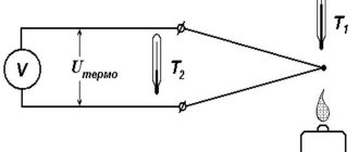
Magnetoelectric MMs are also used for measurements in AC circuits, but only in combination with various AC-to-DC converters. Such devices include, for example, rectifiers and thermoelectric devices.
How digital meters work
Digital electrical measuring instruments have a high accuracy class (the error varies from 0.1 to 1.0%) and a wide measurement range. They are fast and can work together with electronic computers, which makes it possible to transmit measurement results without any distortion over various distances.
These devices are considered comparative and direct evaluation devices. Their work is based on the principle of converting the measured value into code, thanks to which the user has a digital representation of information. What other electrical measuring instruments are considered digital? These are devices that, when measuring a continuous electrical quantity, automatically convert it into a discrete one, encode it and provide the result in a digital form that is convenient for the user to read.
Classification of measuring instruments
According to the principle of operation:
- Indicating - those by which you can only count the measured value at a given time; Self-recording (or recording) - equipped with a device for automatically recording the data of the measured value for subsequent analysis; Signaling - equipped with a special sound or light alarm that is triggered when the device reaches a predetermined value ;Regulating – having the ability to automatically maintain a value at a given level or change it according to a specified law; Installations – performing certain work based on the measurement result according to the set program. They are used for dosing and weighing bulk and liquid substances, sorting products, etc.
By type of readings: analog (continuous) and digital (discrete).
By type of measured quantity: for measuring temperature, electrical indicators, pressure, humidity, gas density, concentration of solutions, flow rate and quantity, as well as for determining the composition (analysis) of liquids and gases.
Devices located in one housing
These are instruments that use one measurement mechanism to measure several quantities non-simultaneously. Or they have several converters with a common reading device (scale) for all. It is calibrated in units of measured quantities. Most often, combined electrical measuring instruments combine devices that measure the strength of direct or alternating current and electrical voltage (ampere-voltmeters); resistance, direct and alternating current, voltage (avometers or ampere-voltmeters). There are also universal digital electrical measuring instruments that measure DC and AC voltage, inductance and the number of pulses.
An example of such a device is the new development of Aktakom ADS-4031. The device harmoniously combines a function generator, a digital oscilloscope, a frequency meter, an RLC meter and a digital multimeter. In addition to the main five combined devices, the oscilloscope tester, thanks to additional accessories, can be used for a number of other measuring tasks.
Device, principle of operation
Electricity consumption of household appliances
Let's look at the operation of electrical devices using the example of basic devices, such as:
- ammeters;
- voltmeters;
- ohmmeters.
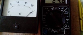
Ammeters
Such devices measure the amount of electric current. Since the readings directly depend on the incoming electrical signal, the ammeter resistance should be less than the load resistance. This is necessary for a constant charge force when connecting a load. According to their design features, such electrical measuring instruments are divided into:
- AC ammeter;
- DC ammeter;
- magnetoelectric;
- electromagnetic.
How does an ammeter work?
An ideal ammeter is a device for measuring electric charge. It is a conductive circuit mounted on an axis between the poles of a permanent magnet. In the absence of a circuit signal, due to spring pressure, the arrow is in the zero position. When the device is turned on, a current pulse is sent to the moving element - the needle deflects by an angle corresponding to the current value. Thus the indicator scale shows the value measured by the device.
There are modifications: with an analogue scale, with a digital scale. In addition, devices differ in division price and measurement limits.
Analog AC voltmeter and digital voltmeters.
Measure voltage:
- permanent;
- variable.
AND
An ideal electrical voltmeter is usually connected to the circuit in parallel. The resistance of a voltmeter is proportional to the signal applied to it. In order to prevent the readings from being affected by distortions of electrical pulses, it is recommended to make its resistivity as large as possible.
There are also digital voltmeters that have digital readouts. The principle of operation of a voltage meter is similar to a current meter, the only difference is in the scale graduations, measurement limits and modifications.
Ohmmeter
A device that allows you to measure both the resistance of an ammeter and the resistance of a voltmeter. Measurement range:
- units, tens (Ohm);
- hundreds, thousands (Ohm).
Such an indicating element is connected to the circuit in series. Measures indirectly the value of resistance, taking into account the value of the incoming electric current and a constant voltage value.
The instrument scale of each electrical device has symbols printed on it, indicating the characteristics of the device, accuracy class (for example, an ammeter), types of operating currents, rated voltage, etc.
An example of a modern resistance meter is the Vitok ohmmeter, which has a combined power supply.
JSC "Electropribor"
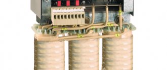
One of these long-livers is the Cheboksary Electrical Instruments Plant. Today it is called Elektropribor OJSC. Its workshops produce analog and digital electrical measuring devices and shunts. The plant's price list includes ammeters, voltmeters, watt and varmeters, and multifunctional measuring devices. As well as measuring converters for voltage, current, frequency and power. In modern realities, the plant has accepted for production a line of auxiliary products - shunts, which are capable of expanding the measurement range of voltage and current. Elektropribor produces transformers and additional resistances.
Devices with electronic converters that measure the frequency of reactive or active power, as well as its coefficient, are in great demand. No less popular are indicators, devices for equipping specialized classrooms, various digital devices and components. At the end of the last century, the company received a certificate confirming the ISO 9001 quality management system, which complies with the international standard.
The Cheboksary plant has been a leader among manufacturers of electrical measuring instruments for more than 55 years.
Definition of electronic devices. Classification of electronic devices (page 1)
1. Definition of electronic devices. Classification of electronic devices
Electronic devices are devices whose operation is based on the use of electrical, thermal, optical and acoustic phenomena in a solid, liquid, vacuum, gas or plasma. The most common functions performed by electronic devices are the conversion of information signals or energy.
The main tasks of an electronic device as a converter of information signals are: amplification, generation, transmission, accumulation and storage of signals, as well as their selection against a background of noise.
Electronic devices can be classified according to their purpose, physical properties, basic electrical parameters, structural and technological features, type of working environment, etc.
Depending on the type of signals and the method of information processing, all existing electronic devices are divided into electrical converters, electric light, photoelectric, thermoelectric, acoustoelectric and mechanoelectric.
Based on the type of working medium, the following classes of devices are distinguished: semiconductor, electrovacuum, gas-discharge, chemotron (working medium is liquid). Depending on the functions performed and purpose, electronic devices are divided into rectifiers, amplifiers, generators, switching devices, indicator devices, etc.
By frequency range – low-frequency, high-frequency, ultra-high-frequency; by power – low power, medium power and powerful.
2. Modes and parameters of electronic devices
The concept of an electronic device mode includes a set of conditions that determine its operation. Any mode is determined by a set of parameters. There are electrical, mechanical, and climatic modes.
Each of these modes is characterized by its own parameters.
The optimal operating conditions of the device during operation, testing or measuring its parameters are determined by the nominal mode. Limit parameters characterize the maximum permissible operating modes. These include the maximum permissible voltage values on the electrodes of the device, the maximum permissible power dissipated by the device, etc. There are static and dynamic modes. If the device operates at constant voltage values on the electrodes, this mode is called static. In this case, all parameters do not change over time. The operating mode of the device, in which the voltage on at least one of the electrodes changes over time, is called dynamic. In addition to the mode parameters, there are also parameters of the electronic device (for example, gain, internal resistance, interelectrode capacitances, etc.). The relationship between changes in currents and voltages on the electrodes in a static mode is described by static characteristics. A set of static characteristics with fixed values of the third parameter is called a family of characteristics.
3.Electrical conductivity of materials.
Semiconductors used in electronics have a monocrystalline lattice. Each atom of the crystal lattice is firmly held at the nodes of the crystal lattice due to covalent bonds. In an ideal lattice, all electrons are bound to their atoms, so such a structure does not conduct electric current. However, small energetic impacts can cause some electrons to be stripped from their atoms, making them able to move around the crystal lattice. Such electrons are called conduction electrons. The energy states of conduction electrons form a zone of energy values (levels) called the conduction band. The energy states of the valence electrons form the valence band. Between the maximum energy level of the valence band W b and the minimum level of the conduction band W c lies the forbidden band. The band gap in Wc determines the minimum energy required to release a valence electron, i.e., the ionization energy of a semiconductor atom. The band gap for most semiconductors is 0.1 – 3 eV.
4. The concept of electrochemical potential (Fermi level).
The probability of finding a free electron in the energy state W is determined by the function
Semiconductors with a donor impurity are called electronic semiconductors, or n-type semiconductors.
With increasing temperature, the Fermi level shifts to the middle of the band gap. In the case of a semiconductor with an acceptor impurity, electrons are minority charge carriers, holes are the majority carriers, and a semiconductor with an acceptor impurity is called a hole or p-type semiconductor.
With increasing temperature, the Fermi level shifts to the middle of the band gap.
5.Inherent conductivity.
Intrinsic and impurity conductivity of semiconductors
1. Features of semiconductors
Structure of semiconductors. In semiconductors, atoms are connected by covalent (pair-electronic) bonds, which are strong at low temperatures and illumination. With increasing temperature and illumination, these bonds can be destroyed, forming a free electron and a “hole”. e) are real particles E
Electronic conductivity is caused by the movement of free electrons.
Hole conduction is caused by the movement of bound electrons that move from one atom to another, alternately replacing each other, which is equivalent to the movement of “holes” in the opposite direction. The “hole” is conventionally assigned a “+” charge. In pure semiconductors, the concentration of free electrons and “holes” are the same. Electron-hole
conductivity - conductivity caused by the formation of free charge carriers (electrons and “holes”) formed when covalent bonds are broken, is called
intrinsic conductivity.
6. Impurity electrical conductivity of semiconductor materials.
Impurity conductivity
– conductivity due to the formation of free charge carriers when introducing impurities of a different valency (n)
Donor impurity
nimpurities > nsemiconductor Arsenic in germanium napprox. =5; np/wire-k=4
Each impurity atom contributes a free electron
n-type semiconductors
with donor impurity
Major charge carriers electrons Non-majority carriers
o –
“holes” Conductivity electronic Acceptor impurity
nimpurities < n semiconductor
Indium to germanium napprox. =3; np/wire-k=4 Each impurity atom captures an electron from the main semiconductor, creating an additional hole.
7. Electrical transitions in semiconductor devices
An electrical transition is a transition layer between regions of a solid with different types or values of conductivity. The most commonly used electrical junction between n- and p-type semiconductors is called an electron-hole junction, or pn junction. Transitions between regions with the same type of electrical conductivity, but with different conductivity values (n+-n; p+-p), are also used. The “+” sign marks an area with a higher concentration of impurities.
Metal-semiconductor junctions are widely used. Electrical junctions can be created either on the basis of semiconductors with the same band gap (homojunctions) or with different widths (heterojunctions).
Electrical junctions are used in almost all semiconductor devices. Physical processes in transitions underlie the operation of most semiconductor devices.
Asymmetrical pn junctions are widely used, in which the concentration of impurities in the emitter is significantly higher than in the other
region - base. In symmetric pn junctions, the concentration of acceptors in the p-region is equal to the concentration of donors in the n-region.
8-9 Electron-hole transition in equilibrium state
Contact potential difference.
Equilibrium corresponds to zero external voltage at the junction. Because the electron concentration in the n-region is much greater than in the p-region, and the hole concentration in the p-region is greater than in the n-region. As a result, charges will diffuse from an area with a higher concentration to an area with a lower concentration, which will lead to the appearance of a diffusion current of electrons and holes.
At the boundary of the p- and n-regions, a layer is created that is depleted of mobile carriers. An uncompensated charge of positive ions appears in the n-type near-contact region, and an uncompensated charge of negative impurity ions appears in the hole region. Thus, the electronic semiconductor is charged positively, and the hole semiconductor is charged negatively.
An electric field of intensity E arises between regions of a semiconductor with different types of electrical conductivity. The resulting double layer of electric charges is called blocking; it is depleted of majority carriers and, as a result, has low electrical conductivity.
The field strength vector is directed in such a way that it impedes the diffusion movement of the majority carriers and accelerates the minority carriers. This field corresponds to the contact potential difference ϕ k, associated with the mutual diffusion of carriers. Outside the pn junction, the semiconductor regions remain neutral. The movement of minority carriers forms a drift current directed towards the diffusion current. So, under equilibrium conditions, the counter drift and diffusion currents must be equal, i.e.
Then the expression for the contact potential difference ϕ k in the pn junction
10. Electron-hole transition in a nonequilibrium state
If a voltage source is connected to the pn junction, the equilibrium state will be disrupted and current will flow in the circuit. There are direct and reverse connections of the pn junction.
10.Direct connection
. Let the external voltage be applied by plus to the p-region, and by minus to the n-region. Moreover, it is opposite in sign to the contact potential difference. Since the concentration of mobile carriers in the pn junction is much lower than in the p and n regions, the resistance of the pn junction is significantly higher than the resistance of the p and n regions. We can assume that the applied voltage drops completely at the junction. The majority carriers will move towards the contact, reducing the carrier deficiency in the pn junction and reducing the resistance and thickness of the pn junction. The flow of major carriers through the contact will increase. The current flowing through the junction is called forward voltage in this case, and the voltage applied to the junction is called forward voltage. The diffusion of holes through the junction leads to an increase in the concentration of holes behind the junction. The resulting hole concentration gradient causes their diffusion penetration deep into the n-region, where they are minority carriers. This phenomenon is called injection. The injection of holes does not violate electrical neutrality in the n-region, since it is accompanied by the arrival of the same number of electrons from the external circuit.
11.Reverse switching
.
If an external voltage is applied plus to the n-region, and minus to the p-region, then it coincides in sign with the contact potential difference. In this case, the voltage at the junction increases, and the height of the potential barrier becomes higher than in the absence of voltage.
The direction of the resulting current is opposite to the direction of the forward current, so it is called reverse current, and the voltage causing the reverse current is called reverse voltage. The field in the transition is accelerating only for minority carriers. Under the influence of this field, the concentration of minority carriers at the transition boundary decreases and a charge carrier concentration gradient appears. This phenomenon is called carrier extraction.
Since the number of minority carriers is small, the extraction current through the junction is much less than the forward current. It is practically independent of the applied voltage and is a saturation current.
Thus, the pn junction has asymmetric conductivity: the conductivity in the forward direction significantly exceeds the conductivity of the pn junction in the reverse direction, which is widely used in the manufacture of semiconductor devices.
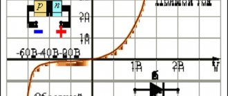
12. Current-voltage characteristic of pn junction
The current-voltage characteristic of a pn junction represents the dependence of the current through the pn junction on the magnitude and polarity of the applied voltage.
13. Properties of pn junction
At large negative voltages in р-n
-transition there is a sharp increase in the reverse current.
This phenomenon is called p-n
junction breakdown.
Transition breakdown occurs when the electric field is sufficiently strong, when minority charge carriers are accelerated so much that they ionize the semiconductor atoms. During ionization, electrons and holes are created, which, accelerating, again ionize atoms, etc., as a result of which the diffusion current through the junction increases sharply, and a jump in the reverse current is observed on the current-voltage characteristic of the p-n
junction in the region of large negative voltages .
It should be noted that after breakdown, the junction fails only when irreversible changes in its structure occur in the event of excessive overheating, which is observed during thermal breakdown. If the power released at the pn
junction is maintained at an acceptable level, it remains operational even after a breakdown. This breakdown is called electrical (recoverable).
14 Design and principle of operation of semiconductor diodes.
Depending on the technological processes used in the manufacture of diodes, there are: alloy, diffusion, planar-epitaxial diodes and their varieties. The structure of a semiconductor diode manufactured using planar epitaxial technology is shown in Fig. 1.
| Rice. 1 |
Most semiconductor diodes are based on asymmetrical pn junctions. Pi-, ni-junctions, metal-semiconductor junctions, p+-p-, p+-n-junctions, heterojunctions are also used as structural elements of diodes. Diodes with p‑i‑n‑, p+-pn - and n+-np structures are also manufactured. The entire structure with electrical transition is enclosed in a metal, glass, ceramic or plastic housing to eliminate environmental influences. Semiconductor diodes are manufactured in both discrete and integrated versions. The main element of a semiconductor diode is p-n
-junction, therefore the current-voltage characteristic of a real diode is close to the current-voltage characteristic
the p-n
I
flowing through the diode on the applied voltage
U
. A typical current-voltage characteristic of the device is shown in the figure.
15. Classification of semiconductor diodes.
Diodes are classified: by material (germanium, silicon, gallium arsenide); transition structure (point, planar); purpose (rectifier, pulse, zener diodes, etc.); frequency range (low and high frequencies); type of current-voltage characteristic, etc. Depending on the technological processes used in the manufacture of diodes, they are distinguished: alloy, diffusion, planar-epitaxial diodes and their varieties. Based on the type of pn junction, planar and point diodes are distinguished. A pn junction is considered planar if its linear dimensions, which determine its area, are significantly larger than its thickness; otherwise, the diode is classified as a point diode. Depending on the area of application, diodes are divided into rectifiers, zener diodes, varicaps, pulse, tunnel, photo, radiative, etc. Based on the type of source material, silicon, germanium, selenium, gallium arsenide diodes, etc. are distinguished. Based on the method of manufacturing the junction: alloy, diffusion, epitaxial, Schottky diodes, etc.
16. Diode symbol system.
To mark semiconductor diodes, an alphanumeric symbol system is used in accordance with OST 11.336.919-81. The first element - a letter or number, characterizes the material used: G (1) - germanium (Ge); K(2) – silicon (Si); A(3) – gallium (Ga) and its compounds; I(4) – indium In and its compounds. The second element, a letter, characterizes the type of diode: D – rectifier; B – varicap; I – tunnel and reversed; C – zener diode and stabilizer; L – emitting LED. The third element is a number that characterizes the purpose of the diode. For example, for group D diodes: 1 – low-power rectifiers (current up to 300 µA); 2 – medium power rectifiers (current up to 10 A); 3 – high power diodes (current over 10 A); 4–9 – pulse diodes with different recovery times. The fourth element (2-3 digits) is the development number (for a zener diode - stabilization voltage in tenths of a volt). The fifth element is a letter, characterizing the option according to its parameters.
1 – general designation (rectifier, pulse, high-frequency diode); 2 – zener diode; 3 – two-anode zener diode; 4 – tunnel diode; 5 – reversed diode; 6 – varicap; 7 – LED; 8 – photodiode |
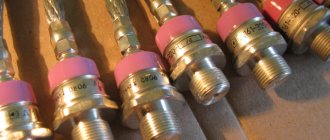
17. Rectifier diodes
Designed to convert alternating current with a frequency from 50 to 20,000 Hz into a pulsating current of one direction and are widely used in power supplies for electronic equipment for various purposes. Silicon, less often germanium and gallium arsenide are used as semiconductor materials for such diodes. The operating principle of rectifier diodes is based on the valve property of the pn junction. They are divided into low, medium and high power diodes. Low power diodes are designed for rectifying currents up to 300 mA, medium and high power - for rectifying currents from 300 mA to 10 A and from 10 to 1000 A, respectively. Advantages of silicon diodes: low reverse currents; Possibility of use at higher ambient temperatures and higher reverse voltages. The advantage of germanium diodes is a low voltage drop of 0.3¼0.6 V when forward current flows (compared to 0.8¼1.2 V for silicon diodes).
Planar, alloy, diffusion and epitaxial diodes made on the basis of asymmetrical pn junctions are used as rectifier diodes. Due to the large area, the barrier capacitance of the junction is large and its value reaches tens of picofarads. Germanium diodes can be used at temperatures not exceeding 70¼80 °C, silicon diodes - up to 120¼150 °C, gallium arsenide - up to 150 °C.
The maximum reverse voltage of low-power low-frequency rectifier diodes ranges from several tens to 1200 V. For higher voltages, the industry produces rectifier columns that use a series connection of diodes. Reverse currents do not exceed 300 µA for germanium diodes and 10 µA for silicon diodes.
Power (power) diodes differ in frequency properties and operate at frequencies in the range from tens of hertz to tens of kilohertz and are made primarily of silicon.
Operation at high currents and high reverse voltages is associated with the release of significant power in the pn junction. Therefore, in installations with medium and high power diodes, coolers are used - air and liquid cooled radiators. In air cooling, heat is removed using a radiator. In this case, cooling can be natural (due to air convection) or forced (using blowing of the device body and radiator using a fan). With liquid cooling, a heat-removing liquid (water, antifreeze, transformer oil, synthetic dielectric fluids) is passed into the radiator through special channels.
The main parameters of rectifier diodes include:
maximum permissible forward current Ipr max;
forward voltage drop across the diode Upr (at Ipr max);
maximum permissible reverse voltage Urev max;
reverse current at a given reverse voltage Irev (at Urev max);
range of operating ambient temperatures;
rectification coefficient Kv;
the limiting rectification frequency corresponding to a decrease in the rectification coefficient by 2 times.
18.
Zener diodes
Semiconductor zener diodes are diodes designed to stabilize the voltage level in a circuit. The operating principle of zener diodes is based on the use of the electrical type of breakdown of the pn junction under reverse bias.
On the reverse branch of the current-voltage characteristic there is a section with a weak dependence of the voltage on the magnitude of the reverse current (a section with electrical breakdown of the pn junction). Planar silicon diodes are used as zener diodes. The current-voltage characteristic of the zener diode is shown in Fig. 5. The magnitude of the reverse voltage at which electrical breakdown begins to develop largely depends on the resistivity of the source material, determined by the concentration of the impurity.
At a voltage of less than 6 V, tunneling breakdown predominates in the pn junction of the diode. In the range from 6 to 12 V, both types of electrical breakdown are observed - tunnel and avalanche, and above 12 V avalanche breakdown predominates. With a change in temperature, the stabilization voltage Ust changes. Low-voltage and high-voltage zener diodes have opposite changes in stabilization voltage with increasing temperature. During a tunnel breakdown, Ust decreases with increasing temperature, and during an avalanche breakdown, it increases. For voltages from 6 to 12 V, the effect of temperature is insignificant, since both types of breakdown exist in the junction.
| Rice. 3 |
The main parameters of the zener diode are:
stabilization voltage Ust – voltage drop across the zener diode when a given stabilization current flows;
minimum Ict min and maximum Ict max currents of the zener diode;
temperature coefficient of stabilization voltage
;
differential resistance of the zener diode, determined in the breakdown area;
static resistance.
Semiconductor diodes used to stabilize voltages less than 1 V using the direct branch of the current-voltage characteristic are called stabistors.
19. Varicaps
Varicaps use the dependence of the barrier capacitance of the pn junction on the reverse voltage. They are divided into tuning, or varicaps, and multiplying, or varactors. Varicaps are used to change the resonant frequency of oscillatory systems. Varactors are used for frequency multiplication.
The main special parameters of varicaps are:
nominal capacitance Sv, measured at a given reverse voltage Urev;
capacitance overlap coefficient - the ratio of varicap capacitances at two given values of reverse voltage;
loss resistance rп – total active resistance, including the resistance of the crystal, contact connections and leads;
quality factor - the ratio of the reactance of a varicap at a given frequency of an alternating signal to the loss resistance;
temperature coefficient of capacitance - the ratio of the relative change in capacitance to the absolute change in ambient temperature that caused it.
In addition to the diodes considered, we produce tunnel diodes, Gunn diodes, avalanche diodes that successfully operate in the ultrahigh frequency range (0.3...300 GHz), as well as photo and emission diodes used in photoelectric and optoelectronic devices and as light-indicating devices.
20. Pulse diodes
Designed to work in digital and other pulse technology devices. Designated in the same way as rectifiers, they have a short duration of transient processes. They differ from rectifier diodes in their small pn junction capacitances (fractions of picofarads) and a number of parameters that determine the transient characteristics of the diode. Reducing capacitances is achieved by reducing the area of the pn junction, so their permissible power dissipation is low (30¼40 mW).
The operation of pulsed diodes is influenced by the effects of accumulation and resorption of charge carriers. When the diode is exposed to short-term pulses, the inertia of the processes of carrier resorption and recharging of its capacity begins to affect. The time to establish the resistance of the directly connected pn-junction of the diode trest is determined by the injection of charge carriers, their diffusion movement deep into the base, which reduces the volume resistance of the diode base to its stationary state. After the end of the rectangular pulse, when the pn junction is switched back on, the value of the reverse current initially sharply increases due to the intensive resorption of nonequilibrium carriers, followed by an exponential decrease to a stationary value of the thermal current I0. The time for recovery of the reverse resistance of the junction tres to its normal value is determined by the formula
, where vdr and vrec are the speeds of drift and recombination of carriers in the structure, which determine the rate of carrier resorption, W is the length of the diode structure between its terminals. The carrier drift speed depends on the field strength, is relatively small and has its own limit vus. To reduce tvos, it is necessary to reduce the volume of the semiconductor structure and increase the rate of recombination of minority carriers, which is achieved by the manufacturing technology of pulsed diodes: by introducing neutral impurities, most often gold (Au), into the source material to create so-called “traps” - recombination centers. The parameters of pulsed diodes are the same as those of high-frequency diodes. In addition, specific parameters are added to them:
ü total capacity of the diode SD (tenths of a unit of picofarad);
ü maximum pulse forward voltage Upr max;
o maximum permissible pulse current Ipr max and;
ü direct voltage establishment time tset – time interval from the moment the forward current pulse is applied to the diode until the specified forward voltage is reached (fractions of nanoseconds¼fractions of microseconds);
ü diode reverse recovery time tres – time of diode switching from a given forward current to a given reverse voltage from the moment the current passes through the zero value until the reverse current reaches the specified value (fractions of nanoseconds ¼ fractions of microseconds).
To reduce tvos, special types of pulsed diodes are used: Schottky barrier diodes (SBD), charge storage diodes (CSD). In the DBS, the junction is made on the basis of a rectifying metal-semiconductor contact, in which the work function from the metal is greater than the work function from the semiconductor. These diodes do not spend time accumulating and dissolving charges in the base; their performance depends only on the speed of the barrier capacitance recharging process. Structurally, DBSs are made in the form of a low-resistance silicon wafer, on which a high-resistivity epitaxial film with electrical conductivity of the same type is deposited. A layer of metal is applied to the surface of the film by vacuum deposition. The inertia of the DBS is mainly determined by the capacitance of the rectifying contact, which can be less than 0.01 pF.
DNZ – used to generate short rectangular pulses. This is achieved due to uneven doping of the diode region. To manufacture such diodes, mesa and epitaxial technology are used.
21. Charge storage diodes (CSDs).
In DNZ the base is made unevenly alloyed along its length. In such diodes, the concentration of impurities in the base decreases as it approaches the pn junction, so the concentration of the majority carriers of the base—electrons—is also uneven if the base has n-type conductivity. Due to this, electrons diffuse towards the pn junction, leaving an excess positive charge of donor atoms deep in the base.
impurity, and near the transition there is an excess charge of electrons. An electric field appears between these charges, directed towards the transition. Under the influence of this field, holes injected into the base when the diode is directly turned on are concentrated (accumulated) in the base at the transition boundary. When the diode is switched from forward to reverse, these holes, under the influence of the field inside the junction, quickly move from the base to the emitter, and the recovery time of the reverse resistance decreases.
To manufacture such diodes, mesa and epitaxial technology are used.
22. Schottky barrier diodes.
diode reverse recovery time tres – time of diode switching from a given forward current to a given reverse voltage from the moment the current passes through the zero value until the reverse current reaches the specified value (fractions of nanoseconds...fractions of microseconds). To reduce tvos, special types of pulsed diodes are used: Schottky barrier diodes (SBD), charge storage diodes (CSD). In the DBS, the junction is made on the basis of a rectifying metal-semiconductor contact, in which the work function from the metal is greater than the work function from the semiconductor. These diodes do not spend time accumulating and dissolving charges in the base; their performance depends only on the speed of the barrier capacitance recharging process. Structurally, DBSs are made in the form of a low-resistance silicon wafer, on which a high-resistivity epitaxial film with electrical conductivity of the same type is deposited. A layer of metal is applied to the surface of the film by vacuum deposition. The inertia of the DBS is mainly determined by the capacitance of the rectifying contact, which can be less than 0.01 pF.
23
Tunnel and reverse diodes
The operating principle of a tunnel diode (TD) is based on the phenomenon of the tunnel effect in a pn junction formed by degenerate semiconductors. This leads to the appearance of a section on the current-voltage characteristic with a negative differential resistance at forward voltage. It is known that a particle that has insufficient energy to overcome a potential barrier can pass through it if, on the other side of this barrier, there is a free energy level that it occupied in front of the barrier. This phenomenon is called the tunnel effect. The narrower the potential barrier and the lower its height, the greater the likelihood of a tunnel transition. The tunnel transition occurs without energy consumption. The current-voltage characteristic of the tunnel diode is shown in Fig. 2.26, a.
2.17. Parameters of tunnel diodes
Peak current I p (from hundreds of microamps to hundreds of milliamps).
Peak voltage U p is the forward voltage corresponding to the current p I.
Valley current Iv, corresponding to voltage Uv.
The valley voltage is the forward voltage corresponding to the current in I. The solution voltage U p is the forward voltage corresponding to the typical current on the second ascending branch of the current-voltage characteristic, determines the possible voltage jump across the load when the tunnel diode is operating in the switching circuit.
24.
A type of tunnel diodes are
inverted diodes
, manufactured on the basis of a semiconductor with impurity concentrations in the p- and n-regions of the diode, lower than in tunnel diodes, but higher than in conventional rectifier diodes.
The current-voltage characteristic of the reversed diode is shown in Fig. 2.28.
The forward branch of the current-voltage characteristic of a reversed diode is similar to the forward branch of a conventional rectifier diode, and the reverse branch is similar to the reverse branch of the current-voltage characteristic of a tunnel diode, since at reverse voltages a tunneling transition of electrons occurs from the valence band of the p-region to the conduction band of the n-region and at low reverse voltages (tens of millivolts) reverse currents turn out to be large. Thus, reversed diodes have a rectifying effect, but the conducting direction in them corresponds to reverse connection, and the blocking direction corresponds to forward connection. Thanks to this, they can be used in microwave detectors and mixers as switches.
| Due to its large volume, this material is placed on several pages: 1 |
JSC "NII Elektromera"
65 years ago, according to the Resolution of the Council of Ministers of the USSR, VNIIEP - the All-Union Scientific Research Institute of Electrical Measuring Instruments was founded. In addition to research work on the development of the latest equipment, small series of high-precision, unique instruments were manufactured here. While developing systems of electrical measuring instruments designed to automate experiments and industrial testing of complex equipment, the institute created measuring and control complexes.
At the end of the last century, VNIIEP was transformed into JSC NII Elektromera.