The NE555 chip, according to its main characteristics, is included in the category of universal timers. The range of time intervals that can be set in them is very wide. Most ne555 circuits contain square-wave pulse generators with different frequencies and lengths. The device, together with a small number of additional radio devices such as resistors and capacitors, is an integral part of various electronics. These are generators, PWM regulator on ne555, temporary ne555 relays, devices for simulating sound with different frequencies, etc.
Pinout NE555
The pinout of the device has not changed for many years, despite being used in different types of applications. The standard version usually has a DIP-8 plastic housing. Surface mounting is done using SOP-8 and SOIC-8.
The first pin is always marked as a small round depression or bulge.
Previously there was an option in a round metal case LM555CH, but it is no longer produced. It consisted of an RS trigger, two comparators, a discharge transistor and an inverting amplifier.
Limits of permissible values
There are a number of typical maximum operating specifications for the NE555. They are found in the most common modifications of this microcircuit. Their differences depend only on the manufacturing company, but, as a rule, are the same in most technical descriptions:
The voltage of the energy source is from 4.5 to 18 Volts.
Power dissipation: 600 microwatts.
The output current is 200 milliamps.
Operating frequency - 500 kilohertz.
Temperature for operation - from 0 to 70 degrees, for storage - from -65 to 150 degrees.
If the specified parameters are exceeded, the device may fail.
Main parameters of the 555 series IC
The product operates properly when the electrical specifications for the signal input and output are maintained. Examples of parameters are summarized in a standard series, where the extreme values show the range and tolerances:
- Voltage level at pin (V) THRES (VCC15) – 8.8–11.2.
- Also at VCC (5V) – 2.4–4.2.
- The current at the THRES pin (A) is 30 x 10-9 and 250 x 10-9.
- The potential at the TRIG pin (V) at VCC15V is 4.5-5.6; VCC 5V 1.1–2.2.
- The remaining operating parameters are in picture 2.
How can I replace NE555?
In Soviet times, there was a complete ne555 analogue of the microcircuit - KR1006VI1. Today it is produced in Latvia and Belarus. The Russian-language instructions for it provide information that fully corresponds to the English version of the ne555 datasheet.
There is one point that is important for selecting a quality replacement. In the specified version of the device there is a priority for the operation of the “stop” outputs over the “start”, but in the original version the situation is the opposite. Most common schemes do not have this functionality, but you should not completely discount it.
Such a microcircuit is an unfinished product with the implementation of 2 operating modes:
Monostable - start timer.
A multivibrator that generates single pulses.
In order for the device to operate in one of these modes, it needs to be slightly improved. For this purpose, an RC circuit is placed between the contacts with a capacitor and resistor selected in advance. Their indicators set the desired frequency ne555 and the periodicity of rectangular signals at the output of the device when power is applied to it. To increase the accuracy of operation in order to avoid external interference, it is necessary to carry out shunting with a capacitance of no more than 0.1 μF.
Manufacturers
Foreign companies producing the NE555 chip and their datasheet: Texas Instruments, Unisonic Technologies, STMicroelectronics, ARTSCHIP ELECTRONICS, NXP Semiconductors, Diodes Incorporated, Fairchild Semiconductor, Harris Corporation, Estek Electronics, Wing Shing Computer Components. On the domestic market you can find products from the following manufacturers: Texas Instruments, STMicroelectronics, Fairchild Semiconductor. Sometimes you can find devices from Unisonic Technologies.
Ne555 - connection diagrams
NE555 operation in timer mode
Requires 2 additional items:
Resistor.
Two containers.
When power is applied, the 3rd leg relative to ground level will have a voltage of 0 Volts. The capacitor that sets the time has no charge, and the circuit can remain in this state for a long time until a positive signal arrives at the second contact. Its value should be three times less than the supply voltage.
When a signal is applied to pin 2, the output of the microcircuit receives a voltage at the supply level. Its length is determined by the charge time C. When this happens, the output voltage decreases to almost zero and the device discharges.
It is important for the circuit that, once it is turned on, no influences on pin 2 change the output voltage level. But it can be reduced by applying a signal to the 4th leg. You can calculate the time interval of the output pulse using the formula: T=1.1*Rt*Ct.
Operation in multivibrator mode
ne555 produces square wave signals. Their periodicity depends on the values of the time-setting RC chain. The design changes slightly, adding additional resistance. Pin 7 connects resistors Ra and Rb, but is switched off inside the timer.
When power is applied to the chip, the output goes high relative to ground, and the capacitor begins charging. When Ct reaches a charge of 2⁄3 of the supply voltage, the circuit switches and the output voltage decreases to 0. Then contact 7 is turned on and the device is discharged.
Advantages and disadvantages
The main advantage of the NE555 microcircuit is its ease of use - to build a circuit, a small harness that can be easily calculated is enough. At the same time, the cost of the device is low.
The main disadvantage of the timer is the pronounced dependence of the pulse duration on the supply voltage. This is due to the fact that the capacitor in a monovibrator or multivibrator circuit is charged through a resistor (or two), and the upper terminal of the resistor is connected to the supply bus. The current through the resistance is formed by the voltage VCC - the higher it is, the greater the current, the faster the capacitor will charge, the sooner the comparator will work, the shorter the generated time interval will be. For some unknown reason, this point is not in the technical documentation, but is well known to developers.
Another disadvantage of the timer is that the threshold voltages of the comparators are formed by internal dividers and cannot be adjusted. This narrows the possibilities for using the NE555.
And one more unpleasant feature. In connection with the push-pull circuit of the output stage, at the moment of switching (when the upper transistor is already open and the lower one is not yet closed, or vice versa), a through current pulse occurs. Its duration is short, but it leads to additional heating of the microcircuit and generates interference in the power circuits.
Main features and disadvantages of the NE555 timer
The main distinguishing feature of the device is the presence of a built-in voltage divider. It sets the upper and lower threshold values at which 2 comparators are triggered. Since it cannot be removed, this limits the applicability of the circuit.
A timer with bipolar transistors has one obvious disadvantage regarding the transition of the output stage between states. When switching, a parasitic through current passes through the device. At its peak it reaches 400 milliamps, which leads to an increase in heat losses.
To solve this problem, you need to install a polarized capacitor. It has a capacitance of no more than 0.1 µF between the wire and the control pin. This stabilizes the device during startup and during operation in general. To make noise immunity even higher, a 1 µF capacitor is included in the power circuit.
Timers based on CMOS transistors do not have these problems. They do not require external installation of capacitors.
KR(F)1006VI1 - programmable timer
| Navigator: QRZ.RU > Amateur radio reference books > Directory of domestic microcircuits |
Housing KF1006VI1 Housing KF1006VI1 Electrical diagram Pin assignments Connection diagrams Electrical parameters Maximum permissible operating modes Recommendations for use Foreign analogues Literature
The microcircuit is a timer for generating voltage pulses with a duration of T=1.1RC (R and C are external timing elements) from several microseconds to tens of minutes.
Designed for use in stable time sensors, pulse generators, pulse width, frequency and phase modulators, voltage and signal converters, key circuits, actuators in control, monitoring and automation systems. Contains 51 integral elements. Housing type 2101.8-1 and 4309.8-A.
Housing KR1006VI1
Case KF1006VI1
Electrical diagram
Pin assignment 1006VI1
1 - general; 2 - launch; 3—output; 4 - reset; 5 — divider control; 6 — operation; 7 - discharge circuit; 8 — supply voltage;
Connection schemes
Electrical parameters
| 1 | Supply voltage | from 3 to 15 V |
| 2 | Low level output voltage at Up=5 V, Uav=3.7...4.7 V, Iout=5 mA at Up=15 V, Uav=11.5...14 V, Iout=0.1 A | no more than 9.35 V no more than 2.5 V |
| 3 | High level output voltage at Up=5 V, Usr=1.8…2.8 V, Iout=0.1 A at Up=15 V, Usr=5.5…8 V, Iout=0.1 A | not less than 2.75 V not less than 12.5 V |
| 4 | Current consumption at Up=5 V, Uav=3.7...4.7 V, Uin=2.3...3.3 V at Up=15 V, Uav=11.5...14 V, Uin=7...9, 5 V | no more than 6 mA no more than 15 mA |
| 5 | Reset current at Up=15 V | no more than 1.5 mA |
| 6 | Output current at Up=15 V | no more than 2 µA |
| 7 | Operating current | 250 nA |
| 8 | Rise (fall) time | 300 ns |
| 9 | Initial error at Up=15 V | no more than 3% |
| 10 | Instability of the initial error from the supply voltage | no more than 0.3%/V |
Maximum permissible operating conditions
| 1 | Supply voltage | 5…15 V |
| 2 | Load current | no more than 100 mA |
| 3 | Power dissipation (50°C) | no more than 50 mW |
| 4 | Ambient temperature | -45…+70 ° C |
| 5 | Permissible value of static potential | 200 V |
Notes: - at an ambient temperature of 50 ° C, the dissipated power is determined by the formula: Pp = 500 mW-5 mW/ ° C (Tamb-50 ° C) - reset current - the value of the current flowing in the timer reset circuit in a given mode - initial error - relative deviation of the duration of the Tx pulse, generated by a timer with given timing elements R and C, from the duration value determined from the expression: Tout = RCln3 - instability of the initial error from the supply voltage - the ratio of the deviation of the initial error of the timer to the change in supply voltage. - maximum reset voltage - the maximum voltage value at the output of the reset circuit, at which a low-level voltage value is provided at the output of the IC.
Recommendations for use
The IC is launched under the condition that U0in is no more than 1/3 of Up, supplied to the “start” pin. To eliminate the instability of the timer start caused by ripple of the power supply, it is recommended to connect a capacitor with a capacity of 1...10 μF in parallel with the power supply in close proximity to the IC pins. The maximum reset voltage is in the range of 0.4...1 V. If the reset pin is not used, it must be connected to pin 8. If the “divider control” pin is not used, it must be shorted to the housing through a blocking capacitor with a capacity of 0.01...0.1 µF. The minimum duration of the pulse generated by the timer is 20 µs. It is not recommended to apply voltage higher than the supply voltage to pins 2,4,6,7.
Foreign analogues
NE555NL, LM555CN-8, LM555M
Literature
Integrated circuits and their foreign analogues
: Directory. Volume 7./A. V. Nefedov. - M.: IP RadioSoft, 1999. — 640 pp.: ill.
Domestic microcircuits and foreign analogues
Directory. Perelman B.L., Shevelev V.I. "NTC Microtech", 1998, 376 p. — ISBN-5-85823-006-7
| Navigator: QRZ.RU > Amateur radio reference books > Directory of domestic microcircuits |
Placement and purpose of pins
The NE555 and transistors that can be used to replace it typically have an eight-lead PDIP8, TSSOP, or SOIC package. The terminals, regardless of the type of housing, are located standardly.
The timer is graphically indicated as a rectangle and labeled as G1 (single pulse generator) or GN (multivibrator).
Types of conclusions:
- GND - common. This is the 1st pin in relation to the key. It is connected to the power supply section of the device with the “-” sign.
- TRIG - launch. When a low pulse is applied to the input of the 2nd comparator, the device starts and a high level signal appears at the output. Their length is affected by the rating of external parts C and R.
- OUT - output. The voltage at a high signal level at the output is 1.5 V, at a low level - 0.25 V. Switching is 0.1 μs.
- RESET - reset. This input has maximum priority. It controls the operation of the device at any voltage on the other terminals. Startup permission is possible at a potential of 0.7 V. Because of this, it is connected to the device’s power supply using a resistor. If a pulse of less than 0.7V appears, the NE555 stops working.
- CTRL - control. Directly connected to the voltage divider, and without external influences, 2/3 Up is supplied. When the ne555 control signal is applied to the pin, signal modulation is obtained. In standard circuits, it is connected to an external capacitor.
Description and scope
NE555 is the development of the American company Signetics, whose specialists did not give up during the economic crisis and were able to bring to life the works of Hans Camenzind. It was he who, in 1970, managed to prove the importance of his invention, which at that time had no analogues. The NE555 IC had a high installation density at low cost, which earned it a special status.
Subsequently, competing manufacturers from around the world began to copy it. This is how the domestic KR1006VI1 appeared, which remained unique in this family. The fact is that in KR1006VI1 the stop input (6) has priority over the start input (2). Imported analogues from other companies do not have this feature. This fact should be taken into account when developing circuits with active use of two inputs.
However, in most cases, priorities do not affect the operation of the device. In order to reduce power consumption, back in the 70s of the last century, the production of a CMOS series timer was launched. In Russia, the field-effect transistor microcircuit was named KR1441VI1.
The 555 timer has found its greatest application in the construction of generator circuits and time relays with the possibility of delays from microseconds to several hours. In more complex devices, it performs the functions of eliminating contact bounce, PWM, digital signal restoration, and so on.
How to make a ne555 metal detector with your own hands
There is a way to make a homemade metal detector from 2 ne555 circuits. They consist of 2 coils:
- Transmissions - Tx.
- Reception - Rx.
The entire structure is divided into 2 blocks. The first one, which is on the left, consists of a square wave generator. The time-setting elements (R1, R2, C1) are selected so that the approximate output frequency is 700 Hz. It is called the frequency of the audible spectrum.
Pulse transmission occurs through a current-limiting resistor - R3. The location of two coils in the same area is such that they together form an overlap and the system has an induction balance. The receive coil voltage is zero, and there is no reaction from the right side of the circuit. If there is a metal object nearby, the balance is disturbed and a sound is heard.
To amplify the signal arriving at the input of microcircuit 2 of the receiving coil, transistor VT1 is used, namely, KT3102EM, or its analogue with any amplification level. The resistors form a voltage amplifier. Using variable resistors, the metal detector is adjusted to ne555. R6 - for adjustment, adjusted after mutual placement of the coils. R7 and R8 help make fine adjustments and are installed in the device housing.
The piezo emitter BA1 is involved in the recognition of the sound signal. It is removed from the unusable multimeter. It is desirable that it has an internal generator. The pulse signal generated at the DD2 output signals and helps to detect small changes in sound when a metal object is nearby.
How to make a reel
To wind the metal detector coils, you need to use an enameled winding wire with a radius of 0.16 mm. Pick up some large object and wrap it around it. The wire can be obtained from an unnecessary electric motor or power transformer.
Take out the wound spool and wrap it with paper adhesive tape. You should get 2 identical coils. Scotch tape is needed because over time the winding loses its shape. It is advisable to make them flattened, resembling the letter D, so that one does not overlap the other. The base for the coils can be a sandwich panel, often used in plastic windows. The coils can be connected to the board using a shielded wire.
Structured integrated circuit inside a chip
So, the process of creating an integrated circuit begins with a single silicon crystal, shaped like a long solid pipe, “cut” into thin disks - plates. Such wafers are laid out into many identical square or rectangular areas, each of which represents one silicon chip (microchip). An example of the internal structure of an integrated circuit, demonstrating the capabilities of such a unique technology for integrating full-fledged electronic circuit solutions.
Thousands, millions, or even billions of components are then created on each chip by doping different areas of the surface into N-type or P-type silicon. Alloying is carried out in various ways. One option is sputtering, when a silicon wafer is “bombarded” with ions of the dopant material.
Another option is vapor deposition, which involves introducing an alloying material in the gas phase followed by condensation. As a result of this introduction, impurity atoms form a thin film on the surface of the silicon wafer. Molecular beam epitaxy is considered the most accurate deposition option.
Of course, the creation of integrated circuits, where hundreds, millions or billions of components are packed into a silicon chip the size of a fingernail, seems to be a very complex process. One can imagine what chaos even a small grain will bring when working on a microscopic (nanoscopic) scale. This is why semiconductors are manufactured in squeaky clean laboratory conditions. The air in laboratory rooms is carefully filtered, and workers must pass through protective airlocks and wear protective clothing.
Who created the integrated circuit?
The development of the integrated circuit is credited to two physicists, Jack Kilby and Robert Noyce, as a joint invention. However, in fact, Kilby and Noyce hatched the idea of an integrated circuit independently of each other. There was even a kind of competition between scientists for the rights to the invention.
Jack Kilby was working at Texas Instruments when the scientist managed to realize the idea of a monolithic principle of placing various parts of an electronic circuit on a silicon chip. The scientist manually created the world's first integrated circuit (1958), using a germanium-based chip. a year later she filed a patent application.
Meanwhile, a representative of the other, Robert Noyce, conducted experiments with miniature circuits of his device. Through a series of photographic and chemical techniques (the planar process), Kilby created a practical integrated circuit just a year later. The production method was also filed for a patent.
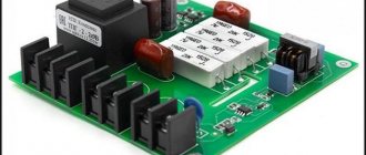
Microcircuits on the board
Diagram of a regular flasher on NE555
This device operates in a multivibrator mode that generates rectangular pulses. Their length is changed by selecting capacitors and resistors. The circuit consists of 2 alternately switched LEDs. But if you only need 1 of them, the second one does not have to be included in the microcircuit; this will not affect the quality of operation of the entire device.
The circuit is powered from 3V, and can range from 3 to 15. When increasing the power, you need to select resistors for the LED circuits. If the power comes from 12 V, the resistors should be 1.5 - 2 kiloOhms.
The assembled flasher does not need to be configured; it works when turned on. It is not necessary to take a 220 kiloOhm resistor; soldering in an alternating or tuning version is enough. This will help you set the LED blinking frequency.
You can use a breadboard to assemble the circuit. Since the number of components in it is minimal, wall-mounted installation can be used. This technique is relevant for motorists.
Device with delay function
Let's move directly to the time relay. In this article we will analyze, on the one hand, a circuit that is as simple as possible, but on the other hand, it does not have galvanic isolation.
The device is dangerous because it contains dangerous voltage. Such a device in its design has 15 elements and is divided into two parts:
- Supply voltage generation unit or power supply unit;
- Node with temporary controller.
The power supply operates on a transformerless principle. Its design includes components R1, C1, VD1, VD2, C3 and VD3. The 12 V supply voltage itself is formed on the zener diode VD3 and smoothed by capacitor C3.
The second part of the circuit includes an integrated timer with a fitting. We described the role of capacitor C4 and resistor R2 above, and now, using the previously stated formula, we can calculate the value of the relay delay time: T = 1.1 * R2 * C4 = 1.1 * 680000 * 0.0001 = 75 seconds ≈ 1.5 minutes By changing the values of R2-C4, you You can independently determine the delay time you need and remake the circuit with your own hands for any time interval. The operating principle of the circuit is as follows. After the device is connected to the network and the supply voltage appears on the zener diode VD3, and, consequently, on the NE555 chip, the capacitor begins to charge until the voltage at inputs 2 and 6 of the NE555 chip drops below 1/3 of the supply, that is, to approximately 4 V. After this event occurs, a control voltage will appear at the OUT output, which will start (turn on) relay K1. The relay, in turn, will close the load HL1.
Diode VD4 accelerates the discharge of capacitor C4 after turning off the power so that after quickly reconnecting the device to the network, the response time is not reduced. Diode VD5 dampens the inductive surge from K1, thereby protecting the circuit. C2 is used to filter interference from the NE555 power supply.
If the parts are selected correctly and the elements are installed without errors, then the device does not need to be configured.
When testing the circuit, in order not to wait a minute and a half, it is necessary to reduce the resistance R1 to a value of 68–100 kOhm.
You probably noticed that there is no transistor in the circuit that would turn on relay K1. This was done not out of economy, but because of the sufficient reliability of output 3 (OUT) of the DD1 chip
The NE555 microcircuit can withstand a maximum load of up to ±225 mA at the OUT output.
This scheme is ideal for monitoring the operating time of ventilation devices installed in bathrooms and other utility rooms. Due to its presence, the fans are turned on only if they are present in the room for a long time. This mode significantly reduces electrical energy consumption and extends the service life of fans due to less wear of rubbing parts.
How to make a ne555 time relay yourself
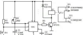
To become more familiar with the timer, make a time relay yourself. This is a simple, classic circuit that anyone can assemble.
To start, toggle switch SB1 is used, and resistor R2 is used to adjust the duration. The approximate operating time of this circuit is 6 seconds. To increase it without changing the characteristics of R2, you need to increase the capacity of C1.
For a daily operating cycle, you need to use a capacitor with a capacity of 1.6 thousand microfarads. When using the microcircuit in conditions close to real ones, the farads can be changed to more appropriate ones for the required working time. For the calculation, use the formula: T=C1*R2, C1 is the capacitance of the selected capacitor, R2 is the average resistance of the adjustment resistor.
The pinout looks like this:
- GND (Ground) - power is reduced.
- Trigger - the contact receives a pulse to start the timer. Occurs when a toggle switch is pressed.
- Output – when the timer is active, an outgoing signal is generated at the contact.
- Reset - A negative signal is given and the timer is stopped.
- Control Voltage - increases the device's resistance to interference.
You can purchase NE555 on Aliexpress (follow the link) and in other online stores at the most affordable prices.