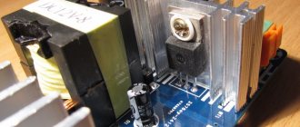
Hello, friends. Let me introduce you to my first laboratory power supply. Every self-respecting radio amateur should have an adjustable power supply to connect various devices. So I decided to build myself a power supply. For the first time I think that unipolar will be enough.
Rice. 1.
Power supply
The power supply is adjustable, from 0 to 30V, maximum current 3A, ripple level 2 - 20mV, has overload protection in the form of current limiting.
↑ How it all began
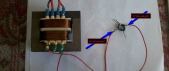
It all started with a transformer. While going through my warehouse supplies, I came across a TPP 248-220-50K transformer. It looks like there should be enough power, I thought and decided to make a power supply. After some digging, I found an old, dirty ammeter. I didn’t want to make large investments in the upcoming project, so I decided to construct it from parts that were available. The measuring device had to be restored:
Rice. 2.
The ammeter is ancient.
Rice.
3. A device in a new way: voltmeter + ammeter
For maximum functionality, I made a double scale, for voltage and current. Without thinking about the transformer voltages, I decided that a voltage of 30 volts and a current of 3 amperes would be enough for my experiments. But this was a correctable mistake; I then rewound the transformer. The case is a tin from an old computer power supply. In old computer power supplies, the fan was small and located at the back near the network connector; my restored voltmeter suddenly took its place.
Rice. 4.
power supply case
surprisingly also fit within the maximum permissible dimensions, a little higher, but when you close the lid nothing is noticeable. The front panel is plexiglass, under it there is a thin sheet of paper with self-adhesive paper on which the inscriptions of the controls are printed on a laser printer.
Rice. 5.
The front panel elements
, a voltmeter, a potentiometer, output terminals and an indication mode switch, tightly pressed this “sandwich” to the body without additional bolts. The result, see Figure 1. After I assembled the front panel, I began to think about the circuit diagram.
Laboratory power supply board, my design and additions. Multi-review.
This text was written not so much for the sake of reviewing the power supply board itself, respected Kirich and other authors succeeded in this, but rather for the sake of describing the design I received as a whole, with the additions necessary, in my opinion, for this power supply in the form of a fan thermal controller and indicator voltage and current, automatic switch of transformer windings, electronic load disconnection, and the power transformer itself and the housing. Some of the devices were purchased on AliExpress, and the other part was assembled from scratch. For the former there will be links, and for the latter there will be diagrams... So, the components used: - A ready-made 150W toroidal transformer, having 2 windings of 12 volts each, purchased in a chip and a dip. Such a transformer was chosen taking into account the possibility of switching windings, dividing the range of output voltages into 2 subranges - 0-11V and everything higher (using either one 12 volt winding or 2 series-connected windings of the same type, giving a total of ~24V). On top of the two factory secondary windings, 2 additional windings were wound. The first is a low-power 13V to power additional devices and a cooling fan. The second winding is more powerful, 7V, wound with a 1.5mm wire (I could have used a thinner one, but I had one), to power a separate 5V USB output connected to a 7805 linear stabilizer; — Design board for laboratory power supply from AliExpress. The set really began to cost a penny - a little more than $5. Flew to Minsk in 29 days, the track was tracked. The board I assembled is pictured above. I only replaced the complete 10,000 µF condenser and the rectifier diodes with Schottky diodes SR560 for a current of 5A. Change operational amplifiers before you start...;
— Ready-made fan controller board with temperature indicator and remote temperature sensor, also from AliExpress.
The temperature controller, costing $1.65, arrived in Minsk in 22 days, the track was tracked. An excellent device, I must say. It can operate in one of two modes - cooling or heating. That is, depending on the selected mode, the thermal controller controls either the heater (turns on if the temperature drops below the set one) or the fan (turns on if the temperature exceeds the set one). To turn off the fan or heater, set the hysterisis value. The controller is controlled using 3 buttons, the values are displayed on a 3-character indicator. There are detailed instructions on the seller's page Instructions
;
— Ready-made voltage and current indicator from AliExpress. Price $3.94. The order took 5 weeks to arrive, the track was not tracked. It should be noted that the indicator turned out to be quite suitable, we will test it later;
— A homemade unit for switching transformer windings (the circuit was found on the Internet). This is perhaps the most important addition to a linear regulated power supply. The fact is that the efficiency of such sources is not very high, especially at low output voltages. So, for example, with an output voltage of 5V and a current of, say, 3A, the output transistor should dissipate about 75W. And in this mode, when the power supply is powered by 24 volts AC (2 windings of 12 volts), the cooling fan, controlled by a thermal controller, almost never turns off. And with an input voltage of ~12V, on the contrary, it turns on very rarely and for a short time. Thus, this addition allows you to significantly improve the operating modes of the power supply, especially considering that I mainly use voltages up to 12V. The only thing is that the solution I have chosen is not the best, because when the voltage decreases, at the moment of switching the windings from two to one (from 24V to 12V), a short dip in the output voltage occurs. The triac circuit is devoid of such a drawback. But for myself, I decided that this nuance is not important to me.
The device is assembled on a breadboard; a rectifier and a 12V voltage stabilizer are located right there, from which the relay, thermal controller and fan are powered. For this stabilizer, an additional low-power winding was wound on the transformer;
— And this is a completely homemade electronic load connection unit, more about it: So, a small technical specification.
— After turning on the power supply, the load must be disconnected, regardless of the last state. — The switched off load should be indicated by a flashing red LED. — A constantly lit green LED should indicate that the load is on. — The load is connected using a relay. — Hardware contact bounce suppression.
The circuit has been corrected, thanks to users IIIap, varicap and alexky who noticed it (wrong polarity of the protective diode). The circuit is built on a cheap Atmel ATtiny2313 microcontroller and a 74HC14 Schmitt trigger. The circuit is powered by 12 volts, which are necessary for the relay to operate. A 7805 linear converter is used to power the microcircuits.
After switching on, the red LED VD2 flashes. The 74HC11 Schmitt trigger allows you to finally and irrevocably get rid of contact bounce. When the button is pressed, LED VD2 goes out and VD1 (green) lights up, at the same time transistor VT1 opens and relay K1 turns on. The next time you press the load and the green LED VD1 are turned off, the red LED VD2 starts flashing. Diode VD1 protects the transistor from voltage surges on the relay coil. The circuit is assembled on a breadboard. If you do not install a Schmitt trigger at the input (and deal with bounce using software), then you need a 10K pull-up resistor on pin 7 of the microcontroller. There are plans to add another control channel to the int0 microcontroller input. The USB output will be controlled.
The control program is written in the Bascom environment.
In the main cycle, the red LED flashes, provided that the PB2 output is low, i.e. the load is disconnected and the green LED is off. When Int1 is interrupted, the Swbutton subroutine is called. The Toggle operator switches the states of the PB2 output (if it was 1, it will become 0 and vice versa). After switching the output, the program returns to the main loop until the next interruption;
The source is under the spoiler
$regfile = "attiny2313.dat" $crystal = 4000000 Config Portb.1 = Output Config Portb.2 = Output Config Pind.3 = INPUT Config Int1 = Falling
Dim Time As Byte
On Int1 Swbutton
Cls
Wtime = 255
Enable Interrupts Enable Int1
Do if pinb.2 = 0 Then Set Portb.1 Waitms Wtime Reset Portb.1 Waitms Wtime Else 'Pinb.4 = 0 End If Loop End
Swbutton: Toggle Portb.2
Return
End
— Relay. On the left is a relay in a blue case, used to turn on/off the load, and a relay in a transparent case, the first group of contacts switches the transformer windings, and the second group turns on the LED indicating the connection of the second winding;
— And finally, the finished case from the old tape streamer. 2Gb DDS cartridges have not been relevant for a very long time, so the device was mercilessly disassembled for spare parts. And the case with its original fan was perfect for my power supply;
This is the front panel. Temporary, because I will redo the layout and the material of the insert will need to be changed (it was white foam plastic - it looks clumsy, but there will be a plug from the computer case, which matches the color of the entire device). But this will happen a little later, when multi-turn resistors arrive from China. A USB connector will also be added. The red regulator is voltage, the blue one is current (the colors of the knobs are selected in accordance with the colors of the indicator segments). The rectangular green LED under the indicator begins to glow when the second winding of the transformer is connected. Above the blue regulator is an LED indicating current stabilization (red). Well, in the area of the output terminals there is a red load connection button and a two-color LED (red-green).
Everything is done on connectors - the front panel is completely removable. The output of the power supply is connected to the front panel via a Deans type connector, which is used for batteries of remotely controlled models;
All components are connected to each other according to the following diagram (corrected, thanks to user MisHel64):
A little assembly:
The winding switch and load disconnect blocks are assembled into a sandwich and installed near the front panel. A load disconnect relay and a fan thermal controller board are installed nearby.
On the inside, a radiator (from some old processor) is screwed to the case fan. A transistor and a thermal controller sensor are screwed to the radiator using thermal paste. Everything is installed in the case from the back.
The main board is mounted on high racks with the parts facing down. Although this arrangement is not the most thermally efficient, there is no other way to place the board and transformer in this case.
I decided to connect the transformer windings using Wago terminals, it turned out very convenient. The wires are a little messy, although they were laid out and tied together with zip ties. Maybe I'll change it later...
And the last component is a 5V stabilizer, mounted on a radiator. And a couple of final photos, a rear view and the assembled power supply. On the back are the power connector, power switch, fuse and switch (blue) for the additional 5V line.
Now let's move on to testing. Let me make a reservation right away that we will be testing not so much the power supply board itself, but the entire assembly assembly. Let's start with the indicator. Under the spoiler there are visual photos of testing. The readings were compared with the reference professional digital multimeter Aktak AM-1095.
Voltmeter reading testing
The ammeter was tested using a 10 Ohm 50 W load resistor. If we remember Ohm’s law, we can easily estimate that with this resistor the current readings should be 10 times less than the voltmeter readings, which we will now verify. We will continue to compare the readings with Aktacom.
Testing ammeter readings
After the measurements, I even began to respect this indicator and I wanted to call it a “device”)).
But it was not possible to get more than 26V from the power supply board at a 10 Ohm load and a current of 2.6A, although at idle the power supply produces 31V.
Testing current stabilization (multimeter, in current measurement mode, directly connected to the output terminals):
Photos
We see that current adjustment is possible up to 3.6A. I finally decided to find out what the output voltage drop would be at almost maximum current. I found two 3.3 Ohm 50 W resistors, connected them in series and connected them to the output terminals - the result is in the photo:
More tests:
Let's compare the voltage at the output of the rectifier with the output. (On the multimeter, the voltage at the output of the diode bridge) On the left without load, on the right with load:
The same thing, but we measure the change at the trance output:
Small conclusions: - the voltage at the trance output drops by 1.6V under load, although the transformer is 150W, and the output is about 80W. - the voltage at the output of the diode bridge drops under the same load, already by 6V. - the output voltage drops by 8.5V at the same load of about 80W. Of course, we need to do something about this... although this operating range is quite enough for me to work with.
Well, all that remains is to measure the ripple, although for linear power supplies this is probably unnecessary and should be done more quickly to emphasize their problem-free nature in this regard, although...
We measure pulsations
I’ll make a reservation right away, because... The block is linear, you shouldn’t pay attention to the frequency meter readings - it measures just about anything... We measure: effective value (minimum readings in the screenshots), maximum peak (average readings) and range (maximum values). 10V, 1A:
10V, 2.1A:
12V, 3.5A:
24V, 3.5A:
everything is beautiful, but there is a nuance: when the block is close to the moment when the voltage begins to sag, i.e. is close to its limit, then wild interference arises from somewhere. In the photo below, only 1 winding of the trance is working, i.e. About 12V AC is supplied to the input of the power supply, and the load of 3A has already reached the limit and there is interference. And if more voltage were supplied to the input, the unit would operate normally. This is a nuance that needs to be taken into account. 10V, 3A:
Purchase Confirmation
In this review, I looked at 3 products I purchased, as well as a couple of useful homemade add-ons. The device turned out to be suitable, but with some nuances. At a minimum, I'll try to replace the output transistor, because... information leaked that the Chinese had them counterfeit. So my first review has come to an end. Express your opinions. Thank you for your attention!
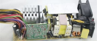
↑ Power supply from inside
The power supply consists of five boards: A1 – 220V presence indicator board (Fig. 6).
A2 – rectifier board A3 – protection board A4 – voltage stabilizer board. A5 – mode indication board. Fragment excluded. The full version is available to patrons and full members of the community.
Board A2 is a block of supply voltages in the power supply; it contains: a rectifier, a transformer winding switching relay, stabilizers and a current sensor. The diode bridge D3-D6 is built on Schottky diodes so that it does not get too hot. As a current sensor, two resistors C5-16MV 0.1 Ohm, voltage stabilizers LM7824, 7805, 7905.
Fragment excluded. The full version is available to patrons and full members of the community.
Board A4 (see Figure 9) contains four LM317s connected in parallel. The LMs are screwed to an aluminum base, which is then connected to the radiator through mica.
Fragment excluded. The full version is available to patrons and full members of the community.
When assembled, the design looks like this (see Figure 10)
Rice. 10.
Power supply without cover
Diagrams of laboratory power supply modules
All power board circuits were designed from scratch, and all printed circuit boards are also independently developed. The first module “Z” is a diode bridge, voltage filtering, negative voltage generation to power the op amps, a 34 VDC positive voltage source for the op amps, powered by a separate auxiliary transformer, a relay used to switch the main transformer windings controlled from another circuit board, and a 5V 1A power supply for power meters.
The “Z” modules of both units were designed to be almost symmetrical (to fit better into the PSU case). Thanks to this, the ARK connectors were placed on one side to connect the wires and heatsink for the bridge rectifier, and the boards, as shown in the pictures, were placed symmetrically.
An 8-amp diode bridge is used here. The main transformers have dual secondary windings, each 14 V and a current of just over 5 A. The power supply was rated for 5 amps, but it turned out that at full voltage 30 V does not produce the full 5 A. However, there is no problem with a 5 amp load at lower voltage (up to 25 V).
The second module is an expanded version of the power supply with operational amplifiers.
Depending on whether the power supply is loaded or in standby mode, the voltage in the region of the amplifier U3, responsible for limiting the current, changes (with the same setting of the potentiometer limits). The circuit compares the voltage across potentiometer P2 with the voltage across resistor R7. Part of this voltage drop is applied to the inverse input of U4. Thanks to this, the output voltage depends on the potentiometer setting and is practically independent of the load. Almost because on a scale from 0 to 5 A the deviation is at the level of 15 mV, which in practice is enough to obtain a stable source for driving the LM3914 circuits that form the LED bar.
The visualization diagram is especially useful when multi-turn potentiometers are used for adjustment. It’s great that with the help of such a potentiometer you can easily set the voltage accurate to the third decimal place. Each LED in the line corresponds to a current of 0.25 A, so if the current limit is below 250 mA, the line is not displayed. The ruler display method can be changed from dot to ruler, but dot is selected here to avoid the influence of too many light dots and reduce power consumption.
The next module is the winding switching system and fan control system that are installed on the radiators of old processors.
The circuits are powered by independent windings of an auxiliary transformer. Here we use m/s op-amp LM358, which contains two operational amplifiers inside. A BD135 transistor is used as a temperature sensor. After exceeding 55C, the fans turn on, and after cooling to approximately 50C, they automatically turn off. The winding switching system reacts to the voltage value at the direct output terminals of the power supply and has a hysteresis of about 3 V, so the relay will not operate too often.
Measurement of load voltage and current is carried out using ICL7107 chips. The meter boards are double-sided and are designed such that for each power source there is a voltmeter and an ammeter on one board.
Useful: Active car subwoofer that can work autonomously
From the very beginning, the idea was to visualize power supply parameters on seven-segment LED displays because they are more readable than an LCD display. But nothing prevents you from measuring the temperature of radiators, winding switches and cooling systems on one Atmega MK, even for both power supplies at once. It's a matter of choice. Using a microcontroller will be cheaper, but as mentioned above, this is a matter of taste.
All auxiliary systems are powered by a transformer that has been rewound by removing all windings except the 220V mains (primary). TS90/11 was used for this purpose.
The secondary winding is wound with 2 x 26 V AC to power the operational amplifiers, 2 x 8 V AC to power the indicators and 2 x 13 V to power the temperature control. A total of six independent windings were created.
↑ Load overvoltage protection
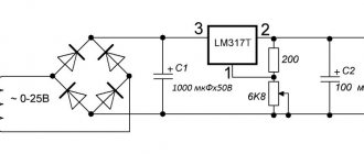
In the classic LM317 connection circuit, a control resistor is connected between the ADJ input and the common wire.
A broken resistor causes the input unstabilized voltage to flow into the load. In the circuit, the output voltage is adjusted using potentiometer R29. Using transistor T5, the load is protected from overvoltage when the slider of potentiometer R29 breaks. Sooner or later a break occurs. In the event of a break, transistor T5 opens through resistor R32 and at the input of ADJ LM317 the potential drops and, as a result, at the output of the stabilizer too. The inclusion of resistor R32 introduces a slight nonlinearity into the voltage regulation using R29. Therefore, its resistance should be as high as possible, but in this regard, you will have to select transistor T5 with the highest gain, otherwise the opening of the transistor may be incomplete.
The output voltage regulation circuit is turned on relative to a negative voltage of -5V. This makes it possible to regulate the output voltage from 0V. Resistor R28 sets the minimum output voltage. The maximum output voltage can be adjusted with resistor R9 on board A2.
Settings
With error-free installation in the control unit circuit, you will only need to adjust the maximum output voltage adjustment range 0: 25 V with resistor R7 and the maximum protection current of 7 A with resistor R8.
The switching unit does not need to be configured. It is only necessary to check the switching thresholds of relays K1, K2 and the corresponding increase in voltage on capacitor C3.
When the circuit is operating in voltage stabilization mode, the green LED (HL2) lights up, and when switching to current stabilization mode, the red LED (HL1) lights up.
↑ Protection of the power supply from overload
On the electrical circuit diagram there are two “grounds” before the current sensor (shunt R8, R12) and after.
The ground to the right, according to the diagram, of the shunt should be taken as the main one, since voltage stabilizers DA2, DA3, and DA5-DA8 are connected relative to it through the negative arm -5V (DA2). This allows you to ignore the voltage drop across the shunt during stabilization. That is, relative to the DA5 stabilizer, the shunt can be attributed to the internal resistance of the voltage source. The power supply's overload protection is a current limiter and is organized on the OP2 comparator (LM339), the distinctive feature of which is an open collector output. The negative input is supplied with a reference voltage from the divider R19, R22 to the positive input - the voltage from the current sensor on resistors R8, R12.
The current limiting value is determined by resistor R19, which can also be placed on the front panel of the device (this can be useful), but I did not do this, since I first designed the case and only then the circuit. During a short circuit, for example, the voltage at the positive input of OP2 becomes lower than at the negative one and the output transistor of the comparator OP2 begins to open, just as T5 begins to lower the potential at the ADJ input of the LM317 stabilizer.
Due to the high gain of the comparator, the current limiting is amazing. 10mA before the limit bar, voltage stabilization is not disrupted. For example, in the experiment I conducted, the short circuit current is 2.94A, with a load of 2.93A the voltage remains stable - when the load is removed, the voltmeter readings do not change.
Schematic diagram
The electrical circuit of the power supply consists of a control circuit, a transformer (T1), a rectifier (VD4 - VD7), power control transistors VT3, VT4 and a switching unit for transformer windings.
The control circuit is assembled on two universal operational amplifiers (op-amps), located in one housing, and is powered by a separate transformer T2. This ensures regulation of the output voltage from zero, as well as more stable operation of the entire device.
To facilitate the thermal operation of power control transistors, a transformer with a sectional secondary winding is used. The taps are automatically switched depending on the output voltage level using relays K1, K2. This allows, despite the high current in the load, to use a heat sink for VT3 and VT4 of relatively small sizes, as well as increase the efficiency of the stabilizer.
The switching unit is designed to, using only two relays, ensure switching of four taps of the transformer; it turns them on in the following sequence: when the output voltage exceeds the level of 6.2 V, K2 is turned on; when the level of 15.3 V is exceeded, K1 is turned on (in this case, the maximum voltage is supplied from the transformer windings).
The specified thresholds are set by the zener diodes used (VD10, VD12). When the voltage drops, the relay is turned off in the reverse order, but with a hysteresis of approximately 0.3 V, i.e., when the voltage drops by this value lower than when turned on, which eliminates chatter when switching windings.
The control circuit consists of a voltage stabilizer and a current stabilizer. If necessary, the device can operate in any of these modes. The mode depends on the resistance of the regulators “I” (R21, R22). The voltage stabilizer is assembled on elements DA3, VT5, VT6.
Rice. 1. Schematic diagram of a laboratory power supply with limiting current adjustment.
The stabilizer circuit works as follows. The required output voltage is set by “coarse” (R9) and “fine” (R10) resistors. In voltage stabilization mode, the voltage feedback signal (-Uoc) from the output (X2) through a divider of resistors R9, RIO, R11 is supplied to the non-inverting input 2 of the operational amplifier DA3.
A reference voltage of +9 volts is supplied to the same input through resistors R3, R5, R7. When the circuit is turned on, the positive voltage at output 12 DA3.1 will increase (it comes to control VT4 through transistor VT5) until the voltage at the output terminals X1 and X2 reaches the level set by resistors R9, R10.
Due to the negative voltage feedback coming from output X2 to input 2 of the DA3.1 amplifier, the output voltage of the power supply is stabilized. In this case, the output voltage will be determined by the relationship:
where Uop = + 9 V.
Accordingly, by changing the resistance of resistors R9 “roughly” and R10 “precisely”, you can change the output voltage (Uout) from 0 to 25 V. When a load is connected to the output of the power source, a current begins to flow in its output circuit, creating a positive voltage drop across resistor R23 (relative to the common wire of the circuit).
This voltage is supplied through resistor R21, R22 to the connection point R8, R12. A negative reference voltage of 9 volts is supplied from the zener diode VD9 through R6, R8.
The DA3.2 operational amplifier amplifies the difference between them. While the difference is negative (i.e., the output current is less than the value set by resistors R23, R24), + 15 V operates at output 10 DA3.2. Transistor VT6 will be closed and this part of the circuit does not affect the operation of the voltage stabilizer.
When the load current increases to a value at which a positive voltage appears at input 7 of DA3.2, there will be a negative voltage at output 10 of DA3.2 and transistor VT6 opens slightly. A current will flow in circuits R16, R17, HL1, which will reduce the opening voltage based on the regulating power transistor VT4.
The glow of the red LED (HL1) indicates that the circuit has entered current limiting mode. In this case, the output voltage of the power supply will decrease to a value at which the output current will have a value sufficient for the current feedback voltage (Uoc) taken from resistor R10 and the reference voltage at the connection point R8, R12, R22 to mutually were compensated, i.e., zero potential appeared.
As a result, the output current of the source will be limited at the level specified by the position of the slider of resistors R21, R22. In this case, the current in the output circuit will be determined by the relation:
where Uop = - 9 V.
Diodes (VD11) at the inputs of operational amplifiers protect the microcircuit from damage if it is turned on without feedback or if the power transistor is damaged. In operating mode, the voltage at the inputs of the op-amp is close to zero and the diodes do not affect the operation of the device.
Capacitor C8 limits the band of amplified op-amp frequencies, which prevents self-excitation and increases the stability of the circuit.
↑ Switching transformer windings
One of the disadvantages of linear stabilizers is low efficiency.
Stabilizers heat up and the greater the difference between the input and output voltages, the greater the heating and, as a result, the loss of power. This problem can be partly solved by reducing the input voltage whenever possible. With an output voltage of 2 volts, there is no point in supplying 30V to the input. But we should not forget about the pulsations of the rectifier. At maximum current, the lower limit of the ripple Umin must be approximately 3 volts higher (for LM317) than the desired output voltage of the stabilizer, otherwise the ripple will pass to the output of the stabilizer. You need to monitor this with an oscilloscope, since multimeters show the average value of the ripple voltage, you might think that stabilization for some reason is not working, but in fact there will be a slight ripple at the output.
On comparators OP1, OP3, OP4 and relays K1, K2, K3, switching of the transformer windings is organized. The positive inputs of the comparators are supplied with the output voltage of the power supply through dividers R20 and R21, R30 and R31, R38 and R39. The negative inputs are reference voltages that determine the relay response levels. Resistors R15, R24, R34 introduce a small (0.1V) hysteresis into the operation of the comparators, this ensures clear opening of the transistors at the same comparator input voltages.
The relays are selected for 24V, the contacts are 16A, the relay coil consumes 17mA. Therefore, a half-wave rectifier based on diode D2 and capacitor C9 is quite sufficient for power supply. As relay keys, I decided to take low-voltage computer mosfets Q25SN03A -T1-T3, drain-source voltage 30V. They can usually be removed from the faulty motherboard in the processor power area. During development, there was a breakdown of the gate of one of the switches, after which I installed zener diodes D7, D8, D10 parallel to the gates of the transistors.
When the relay was turned off, the oscilloscope recorded a spike on the drain at 40V; perhaps the gate had broken through some stray capacitors. But after installing the zener diodes, the flight is normal. By the way, these transistors may not be the best option for switching relays. When K2 is turned on, there is no point in keeping relay K1 turned on; for this, transistor T4 bypasses the gate of transistor T3, relay K1 does not turn on, thereby saving precious 17 mA.
In general, for an output voltage of 30V it is not at all necessary to make 3+1 input voltages; I think two relays and three windings would be enough. But it was problematic to wind three windings when rewinding the transformer, I wound it with a 1.2 mm wire and one 7 Volt winding was placed in one layer, I didn’t dare to make one and a half layers, since it might not fit into the window. Switching the windings is a personal matter, if the radiator allows it, we can assume that the power supply has an additional function - heating the apartment, and the efficiency can be taken as 100%.: smile:
Electronic switch of the secondary windings of a laboratory power supply.
There are many different schemes for switching the taps of the secondary windings of a transformer in laboratory power supplies, to reduce the power dissipation of power supply transistors, and to increase the efficiency of power supplies at low output voltages. There are circuits of “switches” using relays, and electronic versions using triacs, such as the one in the figure below.Triacs are connected to the secondary winding of the power transformer at such a switch in the following (or similar) way.
All of these schemes have their own specific disadvantages. Non-relay circuits make clicking noises, and relay contacts do not last forever, especially in current stabilization (limiting) mode. There is no such drawback in a circuit based on triacs; it works quite stably, but... there are times when the triacs are knocked out, especially with a powerful transformer. Either one triac does not have time to close when the second one has already opened, or there are some other reasons, but the fact remains that triacs are sometimes knocked out with a whistle. All these shortcomings are most likely due to the fact that the windings are switched with interruption of the current. To get rid of these shortcomings, you need to avoid interrupting the current, that is, do not interrupt the current in the load, but add or reduce the input voltage to the power supply.
Below we present to your attention a diagram of an electronic switch for the secondary windings of a transformer, made using thyristors and devoid of these disadvantages. For example, it can be used in a laboratory power supply with an output voltage of 0-35 volts. I’ll say right away that this idea is not mine, but suggested by kotosob
- from the forum of the Soldering Iron site, I am only offering my version of the implementation of this idea. For this circuit, it makes absolutely no difference at what point in the half-cycle the thyristors are turned on and at what time the voltage on the rectifier becomes higher or lower. In this circuit, thyristors play the role of controlled rectifier diodes, which, when turned on, replace and turn off the bridge rectifier diodes, or opened thyristors with a lower output voltage. The number of rectifier cells can be reduced or increased, depending on needs.
Diagram of an electronic switch for secondary windings.
The circuit works as follows; If the output voltage of the power supply does not exceed 7.5 volts, then all zener diodes (ZD1-ZD3) and, accordingly, thyristors are closed, and the voltage to the diode bridge is supplied from the first part (II) of the secondary winding of the power transformer. When the output voltage of the power supply increases above 7.5 volts, the zener diode ZD1 opens and, naturally, the transistor VT1 opens. The load of the transistor is the LED of the triac optocoupler, which unlocks the triac of the optocoupler, and that in turn unlocks the thyristors VS1, VS2. Thyristors begin to work as rectifier diodes, and since their output voltage exceeds by 8 volts (minus the drop voltage across the thyristors) the output voltage supplied to the upper arm of the diode bridge, the latter simply turn off and the output voltage of the rectifier increases. With a further increase in the output voltage of the power supply, the following zener diodes and, accordingly, thyristors open and the output voltage supplied to the filter capacitors increases. When the output voltage of the power supply decreases, everything happens in the reverse order. The zener diodes and, accordingly, the accompanying thyristors close, and the voltage supplied to the filter capacitors decreases. The switching thresholds here are selected at the following output voltages of the power supply - 7.5; 15; 22.5 volts, and depend on the zener diodes used. Accordingly, the voltages supplied to the input of the power supply are 8, 16, 24, 32 volts (without taking into account the voltage drop across the rectifier elements). The circuit is designed to use thyristors. Any thyristors with the required output current and permissible voltage can be used in the circuit, and if they are not available, then any triacs can be installed. When using the latter, resistors R1-R6 must be excluded. And if you use triacs of the VTA series, then they must be selected with a maximum current - no less than 2-3 times the maximum output current of the power supply.
When using triacs, in order for the circuit to work properly, the following must be observed; Triacs are switched on instead of thyristors as follows - the 2nd anode of the triac according to the datasheet - in place of the anode of the thyristor according to the diagram, -1st anode of the triac according to the datasheet - in place of the cathode of the thyristor according to the diagram. It is best to use thyristors (and triacs) in insulated cases so that they can be installed on a common radiator. You can also use any optocouplers, transistors and diodes, depending on what is available. The secondary winding of the power transformer contains taps (sections) for the required output voltage and is wound with a wire with a cross-section in accordance with the required load current. In the described circuit, all sections of the secondary winding are identical and have an output voltage of 8 volts. You can completely choose at your own discretion the switching thresholds, the number of sections (taps) of the secondary winding of the transformer and the number of rectifier cascades (cells) you need. The circuit is powered by an additional source with an output voltage of 5 volts. You can use an additional source with an output voltage of 5-24 volts, but in this case it will be necessary to select resistors in the collector circuits of the transistors so that when the transistor opens, the current through the optocoupler LED does not exceed 10-15 mA.
Yes, the described circuit has hysteresis, since the zener diodes here open smoothly. For simple power supplies, this is quite acceptable, but where a power supply with current stabilization and rapid changes in voltage across the load is needed, it is best to replace the zener diode circuit with a comparator circuit and set the hysteresis to within 0.5 volts.
↑ Tests
The first thing that comes to mind when checking a power supply is to check the quality of the output voltage. To begin with, the constant load is incandescent light bulbs. Current 2.9A Voltage 9V.
Rice. 12
Oscillograms 2.9A 9V
From the oscillogram in Figure 12 it can be seen that low-frequency ripples are not observed.
A small high-frequency noise penetrates from the outside and does not disappear even when the power supply is turned off; if you turn on a nearby computer, the noise increases sharply and emissions of the pulse generator appear, but they are negligible. Perhaps it was necessary to put a filter in front of the transformer. I decided to use my old ASUS Z99H laptop as a dynamic load. Power supply 19V Current consumption fluctuates within 1 - 2 A. For comparison, Figure 13 shows idling without a load of 19V.
Rice. 13
Oscillogram 19V, idle, AC isolation
Figure 14 shows ripples when the laptop is running. The ripples are small with the operating frequency of the laptop's internal switching power supply being 100KHz.
Rice. 14
Oscillogram 19V, load 1-2A, AC isolation
↑ Disadvantages
The main shortcoming of my power supply that I have identified is the case, it is too small.
If you have more space, you could combine board A2 and A3, if you wish, put a small fan inside, and a larger transformer, if available, would fit into a larger case. My transformer is of course rather weak, 3 A without ripple was achieved only at 28.5V. At 30V, pulsations creep to the output, as always, I didn’t have enough turns, but even if I had enough, nothing good would have happened, since 90 Watts is its maximum power and with prolonged use it will heat up, the wax with which I impregnated the trans I feel it will flow.
The next drawback is the measuring device; moreover, it cannot simultaneously display current and voltage, so it entails a current sensor of relatively high resistance, which heats up a little at a current of 3A, the situation is aggravated by poor ventilation in the case. As a result of heating, the shunt resistance changes and my ammeter begins to lie a little, but this is not critical for me.
For those who decide to repeat the circuit, I recommend not to repeat my mistakes and not to spare resistors for the shunt. Choose a transformer with a power reserve, and use a more modern voltmeter and ammeter, digital for example. The shortcomings I have listed, in principle, do not relate to the circuit design, so I am satisfied with my work.
Laboratory transformer control unit
A radio amateur often requires adjustable AC voltage. It is usually obtained using a laboratory adjustable autotransformer (LATR). Unfortunately, the LATR output has a galvanic connection to the network, and its movable electrode (slider) often burns out. In addition to damage to the slider itself, this can also lead to winding failure. And the price of a good LATR is very high, and few people can make it themselves.
There is a long-known way to regulate the voltage on the load using not an autotransformer, but a regular transformer with several secondary windings switched by switches. Such a transformer is described, for example, in the article by A. Terskova “In steps of one volt” (“Radio”, 1993, No. 9, pp. 24, 25). Its output is not galvanically connected to the network, and the output voltage can be adjusted in 1 V steps from 0 to 255 V.
Unfortunately, the constant need for calculations for the correct switching of the secondary windings of such a transformer to the required voltage makes it difficult to use. There is no need to talk about a monotonous increase or decrease in voltage in small steps. But the main drawback of this solution is that installing just one switch in the wrong position can damage the load, especially low-voltage ones.
To prevent such troubles, as well as to simplify the use of the transformer, the device presented below has been developed. The goal was to use parts that would probably be found in a radio amateur's inventory. The block can be simplified, but this will be discussed later.
The diagram of a laboratory transformer (without a control unit) is shown in Fig. 1. It differs from the diagram from the above-mentioned article by A. Terskov only in that manual switches are replaced by electromagnetic relays. Their contact groups K1.1-K8.1 are connected in such a way that when the windings of all relays are de-energized, there is no voltage at the output. This is done so that during transient processes that occur when the transformer is connected to the network, voltage does not appear at the output. The maximum voltage (255 V) at the output will only be if all relays are activated.
Rice. 1. Diagram of a laboratory transformer (without control unit)
Unlike the original, transformer T1 has an additional winding X with a diode rectifier bridge VD1 for powering the relay windings and an integrated voltage stabilizer DA1 for powering the control unit microcircuits.
The control unit, the diagram of which is shown in Fig. 2, assigns to each of the possible values of the output voltage (from 0 to 255 V in steps of 1 V) an eight-bit (according to the number of relays switching the windings) binary code. A one in any digit of this code means that the corresponding relay should operate, zero means that it should release the armature.
Rice. 2. Control unit diagram
When the voltage on the primary winding of the transformer is 230 V, the output voltage in volts is equal to the number set by pressing the SB1 and SB2 buttons on the HG1-HG3 indicators. During operation, there is no need to think about the correct switching of the secondary windings, which increases the convenience and efficiency of setting the required output voltage.
It should, however, be noted that the control unit does not measure the output voltage, but only shows its “theoretical” value on the indicator. For this reason, if the network voltage differs from the nominal one and under the influence of the load, the actual output voltage may differ from the value shown by the indicators.
Conventionally, the control unit can be divided into several functional units. This is a reverse counter on DD2-DD4 chips with the logic that controls it on the DD1 chip, a code converter on the DS1 RPOM chip, an indication unit on DD5-DD7 chips.
A pulse generator with a frequency of about 2 Hz is built on the DD1.1 logic element. Element DD1.4 inverts the generator signal. Inversion is needed so that the counters DD2-DD4 change state when the SB1 and SB2 buttons are pressed and not when the SB2 buttons are released.
Adjust the voltage using buttons SB1 (towards a decrease) and SB2 (towards an increase). Circuits R1C3 and R3C4 suppress bouncing of button contacts. While none of the buttons is pressed, the control input of the generator (pin 1 of DD1) is set to a low logic level. When you press the SB1 button, a high level voltage is supplied to this input through resistor R9 and decoupling diode VD4. After some time the generator starts. If the button is pressed briefly, the generator will not start, but a single pulse will appear at its output in response to each press. With each pulse, the counter contents decrease by one.
In order to avoid their sudden transition to state 999 when the counters reach the zero state, when zero is reached, the operation of the generator is blocked through the diode VD6 by the low logical level of the overflow signal from pin 7 of the counter DD4. Further, starting the generator is possible only with the SB2 button. The operation of this button is similar, but, in addition to starting the generator, it supplies a high level to the counting direction control inputs (pins 10) of counters DD2-DD4. Upon reaching the maximum value of 255, the voltage level at the output of element DD1.3 becomes low and, through diode VD3, blocks the operation of the generator.
Since the device should not respond to simultaneous pressing of both buttons, a blocking unit is introduced into it (resistors R2, R6, R7). The voltage from resistor R2 is applied to the counting enable input (pin 5) of counter DD2. If both buttons are pressed, this voltage level becomes high, which prohibits pulse counting.
Circuit R11C12 serves to reset counters DD2-DD4 when supply voltage is applied. You can reset them at any time by pressing the SB3 button. Since the outputs of 9 counters are connected to a common wire, the counters operate in decimal mode, generating at the outputs a three-digit decimal number in BCD code - the specified output voltage value. This number is sent to the address inputs of the DS1 PROM. Each value of the output voltage corresponds to a memory cell in which the binary equivalent of a binary decimal number is written. For example, at address 10 0011 0000 (the binary decimal representation of 230) the code is 11100110 (the binary number equal to decimal 230).
The code from the outputs of the DS1 RPOM is fed to electronic keys assembled on transistors VT1 -VT8 and control relays K1-K8. In Fig. Figure 2 shows a diagram of only one key, the rest are identical. Switches on discrete transistors can be replaced with a KR1109KT63 (ULN2803A) microcircuit containing eight such switches.
The number from the counter outputs is also sent to the display unit, which consists of binary-decimal code converters into “seven-element” DD5-DD7 and LED indicators HG1-HG3. The HG3 indicator shows units, HG2 - tens, and HG1 - hundreds of volts.
The VT9 transistor has a unit for extinguishing the insignificant zero in the most significant digit of the indicator. The collector of this transistor is connected to the indication blanking input of the DD7 code converter. If counter DD4 contains the number 1 or 2, then a high level voltage is supplied to the base circuit of transistor VT9 through diode VD18 or VD19, the transistor is open, and the HG1 indicator is on.
Similarly, on transistor VT10, a unit for extinguishing an insignificant zero on the HG2 indicator is built. If the number in counter DD3 is different from zero, a high level voltage is supplied to the base of transistor VT10 through diodes VD20-VD23. A low logic level on the VT10 collector allows the operation of the DD6 code converter and the HG2 indicator. If the meter DD3 is zero, but the transistor VT9 is open (in the meter DD4 1 or 2), then a low-level voltage is supplied to the indication blanking input of the code converter DD6 through the diode VD24 from the collector of the transistor VT9.
The VD18-VD23 diodes could be abandoned by supplying signals from the overflow outputs of the corresponding counters to the base circuits of transistors VT9 and VT10, but in this case the extinguished insignificant zeros will flash when the SB2 button is pressed.
If desired, the indication unit can be eliminated, and an AC voltmeter with a measurement limit of 300 V can be connected to the output of the transformer. In this case, the RPOM chip and the DD4 counter can also be removed, and the remaining two can be switched to operate in binary mode. In this case, signals to the transistor switches that control the relays should be supplied from the outputs of the meters. The accuracy of setting the output voltage with this simplification will depend on the error of the voltmeter.
A printed circuit board for the control unit has not been developed, but some of the nodes can be placed on the printed circuit boards shown in Fig. 3 and fig. 4. They were once developed for other devices, but are also suitable for the one presented in the article. The remaining elements can be mounted on a breadboard by connecting their pins with a mounting wire. Blocking capacitors C5-C10 are installed directly on the power pins of the microcircuits. Please note that in fig. 3 the numbers of connection points of the indication board to the meter outputs are highlighted in color. These numbers coincide with the wire numbers of the corresponding harness in the diagram in Fig. 2.
Rice. 3. Control unit printed circuit board
Rice. 4. Control unit printed circuit board
The device uses MLT resistors, all capacitors are imported. Instead of KT315G transistors, you can use any transistors of the same series. In addition, transistors KT315G (VT1-VT8) can be replaced with 2SC945, and the rest - with any low-power npn transistors. KD522A diodes can be replaced with KD521, KD510 with any letter indices or with 1N4148. Replacing KD243V diodes with widely used 1N4007 diodes. The possibility of replacing microcircuits of the K176 and K561 series with their imported analogues has not been tested. The KR573RF5 microcircuit must be programmed before installation in the device. It can be replaced with an imported series 2716 or 27С16.
Buttons and switches can be anything. The relays are imported RAS-1215, they can be replaced with others with an operating winding voltage of 12 V and with switching contacts capable of switching the required load current. The winding resistance of the relays used is 400 Ohms.
Transformer T1 can be wound according to the recommendations of A. Terskov, but with an additional winding X for a voltage of 10 V, wound with a wire with a diameter of at least 0.4 mm. But instead of a PL 25x50x100 magnetic core, it is better to use an SL magnetic core of a similar cross-section - it is much easier to wind the windings not on two, but on one frame.
Setting up the device consists of selecting, if necessary, the frequency of the generator on element DD1.1. With the element ratings indicated in the diagram, it is about 2 Hz. This frequency should not be set too high, since the relay contacts will spark strongly and burn. It is also advisable to check that the ROM is programmed correctly. When setting the output voltage value on indicators HG1-HG3, a binary code of this number should appear at the outputs of the DS1 RPOM.
If necessary, you can speed up the voltage setting by introducing an additional switch SA1 and button SB4 according to the diagram shown in Fig. 5. With the SA1 switch position shown on it, the device operates as usual. When you enable the quick installation mode, all relays will be turned off, which will make the voltage at the transformer output zero. Using the SB4 button, connect resistor R35 in parallel with resistor R5, thereby increasing the frequency of the generator by approximately five times. Now you can quickly set the desired value on the indicator, and then, returning to normal mode, obtain the required voltage at the output.
Rice. 5. Connection diagram for switch SA1 and button SB4
The operation of a transformer with the described control unit is accompanied by such an unpleasant phenomenon as burning of the relay contacts (which, however, affects both the LATR slider and the switches). If the transformer load contains an inductive component (for example, a motor or another transformer), then it may be necessary to bypass the relay contacts with protective RC circuits (not shown in the diagram in Fig. 1). Alternatively, you can set the voltage without a load, and connect the load after, then there will be no burning of the contacts.
In conclusion, I note that the use of the described control unit is not limited only to a laboratory transformer; it can be used, for example, in a power supply. In this case, only the primary winding, secondary windings II-VII and X and five relays (K1 - K5) should be left on the transformer. It will be possible to set the voltage from 1 to 31 V in 1 V steps, which is quite enough for most laboratory power supplies.
DS1 RPOM programming files in several formats with the same content can be downloaded here.
Author: E. Gerasimov, village of Vyselki, Krasnodar Territory