The author of the article is a professional tutor, author of textbooks for preparing for the Unified State Exam Igor Vyacheslavovich Yakovlev
Topics of the Unified State Examination codifier: semiconductors, intrinsic and impurity conductivity of semiconductors.
Until now, speaking about the ability of substances to conduct electric current, we have divided them into conductors and dielectrics. The resistivity of ordinary conductors is in the Ohm m range; The resistivity of dielectrics exceeds these values on average by orders of magnitude: Ohm m.
But there are also substances that, in their electrical conductivity, occupy an intermediate position between conductors and dielectrics. These are semiconductors
: their resistivity at room temperature can take values in a very wide range of Ohm m. Semiconductors include silicon, germanium, selenium, and some other chemical elements and compounds (Semiconductors are extremely common in nature. For example, about 80% of the mass of the earth's crust is made up of substances that are semiconductors). The most widely used are silicon and germanium.
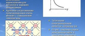
The main feature of semiconductors is that their electrical conductivity increases sharply with increasing temperature. The resistivity of a semiconductor decreases with increasing temperature approximately as shown in Fig. 1.
Rice. 1. Dependence for a semiconductor
In other words, at low temperatures semiconductors behave like dielectrics, and at high temperatures they behave like fairly good conductors. This is the difference between semiconductors and metals: the resistivity of a metal, as you remember, increases linearly with increasing temperature.
There are other differences between semiconductors and metals. Thus, illumination of a semiconductor causes a decrease in its resistance (and light has almost no effect on the resistance of the metal). In addition, the electrical conductivity of semiconductors can change greatly with the introduction of even minute amounts of impurities.
Experience shows that, as in the case of metals, no transfer of substance occurs when current flows through a semiconductor. Therefore, the electric current in semiconductors is due to the movement of electrons.
A decrease in the resistance of a semiconductor when it is heated indicates that an increase in temperature leads to an increase in the number of free charges in the semiconductor. Nothing like this happens in metals; therefore, semiconductors have a different mechanism of electrical conductivity than metals. And the reason for this is the different nature of the chemical bond between the atoms of metals and semiconductors.
Covalent bond
The metallic bond, as you remember, is provided by a gas of free electrons, which, like glue, holds positive ions at the nodes of the crystal lattice. Semiconductors are structured differently - their atoms are held together by covalent bonds.
. Let's remember what it is.
Electrons located in the outer electronic level and called valence
, are weaker bound to the atom than the remaining electrons, which are located closer to the nucleus.
In the process of forming a covalent bond, two atoms contribute one of their valence electrons “to the common cause.” These two electrons are shared, that is, they now belong to both atoms, and therefore are called a common electron pair
(Fig. 2).
Rice. 2. Covalent bond
A socialized pair of electrons is what holds the atoms near each other (using the forces of electrical attraction). A covalent bond is a bond that exists between atoms due to shared electron pairs
.
For this reason, a covalent bond is also called pair-electronic
.
Crystal structure of silicon
Now we are ready to take a closer look at the internal structure of semiconductors. As an example, consider the most common semiconductor in nature—silicon. The second most important semiconductor, germanium, has a similar structure.
The spatial structure of silicon is shown in Fig. 3 (picture by Ben Mills). The balls represent silicon atoms, and the tubes connecting them are channels of covalent bonds between the atoms.
Rice. 3. Crystal structure of silicon
Note that each silicon atom is bonded to four
neighboring atoms. Why does this happen?
The fact is that silicon is tetravalent - there are four valence electrons on the outer electron shell of the silicon atom. Each of these four electrons is ready to form a shared electron pair with the valence electron of another atom. This is what happens! As a result, the silicon atom is surrounded by four atoms docked to it, each of which contributes one valence electron. Accordingly, there are eight electrons around each atom (four of our own and four of others).
We see this in more detail on a flat diagram of a silicon crystal lattice (Fig. 4).
Rice. 4. Silicon crystal lattice
Covalent bonds are depicted as pairs of lines connecting atoms; These lines contain common electron pairs. Each valence electron located on such a line spends most of its time in the space between two neighboring atoms.
However, valence electrons are by no means “tightly tied” to the corresponding pairs of atoms. There is an overlap of the electron shells of all
neighboring atoms, so that any valence electron is the common property of all neighboring atoms.
From some atom 1, such an electron can go to its neighboring atom 2, then to its neighboring atom 3, and so on. Valence electrons can move throughout the entire space of the crystal - they are said to belong to the entire crystal
(and not to any one atomic pair).
However, silicon's valence electrons are not free (as is the case in the metal). In a semiconductor, the bond between valence electrons and atoms is much stronger than in a metal; Silicon covalent bonds do not break at low temperatures. The electron energy is not enough to begin an ordered movement from a lower potential to a higher one under the influence of an external electric field. Therefore, at sufficiently low temperatures, semiconductors are close to dielectrics - they do not conduct electric current.
Semiconductor manufacturing
It's no secret that an important indicator of the degree of development of the semiconductor industry in a country is the level of mastered technological standards. Thus, the Chinese company SMIC is currently actively mastering the 14 nm technological process, and the Taiwanese TSMC is already producing products at 7 and 5 nm. South Korea is keeping pace with TSMC and is also manufacturing products with 7 nm topology, while simultaneously mastering 5 nm technology. At the same time, the US has a 5nm fab planned for 2024-2029, and Intel is in the 7nm race but is facing challenges, announcing in July 2022 that next-generation chip production will be delayed until 2021. Thus, Samsung (South Korea) and TSMC (Taiwan) are currently considered the most advanced factories in the field of semiconductor production. These industry leaders are planning a transition to a 3 nm topology by the mid-2020s [9].
On the Russian market, Mikron PJSC has mastered the 90 nm process technology, which corresponds to the level of semiconductor technology achieved in the world in 2002–2003 (Intel Pentium 4, Prescott).
The company has also mastered the 65 nm technological process for development and development purposes. To reduce the mastered level of topological standards, in January 2022, Russia approved the construction of factories capable of producing chips with a topology of 28 nm and below (down to 5 nm). The creation of the first factory with a 28 nm topology is being discussed on the basis of the Angstrem-T enterprise, but there is still a question about the supply of equipment for the factory in connection with the sanctions policy [10]. While technologies are being mastered, all developers of domestic chips (Elbrus, Baikal, etc.) are forced to order production abroad. The table provides summary information on semiconductor production in the context of topological capabilities available to countries. Table. Semiconductor production in terms of topological capabilities available to countries
| Topology (NM) | 180 | 130 | 90 | 65 | 45/40 | 32/38 | 22/20 | 16/14 | 10/7 | 5* (small series) |
| USA | 24 | 18 | 11 | 8 | 4 | 4 | 4 | 4 | 2 (Intel (10 nm)) | |
| South Korea | 4 | 4 | 3 | 2 | 2 | 2 | 2 | 2 | 2 (Samsung, SK Hynix) | 1 (Sumsung) |
| Taiwan | 9 | 9 | 6 | 6 | 6 | 6 | 5 | 3 | 1 (TSMC) | 1 (TSMC) |
| Japan | 18 | 10 | 7 | 6 | 5 | 1 | 1 | 1 (Kioxia) | ||
| China | 19 | 18 | 16 | 13 | 8 | 6 | 3 | 1 (SMIC) | 1 (SMIC) | |
| Other | 20 | 13 | 5 | 1 | 1 | 1 | 1 | 1 | 1 (GF) | |
| Total | 94 | 72 | 48 | 36 | 26 | 20 | 16 | 12 | 7 | 2 |
Note. Some of the companies listed in the table above have manufacturing facilities located in countries other than their headquarters but are included in the country totals. China's SMIC is listed as having sub-10nm technology, although it is still just trying to master it. Source : Triolo P., Allison K., The geopolitics of Semiconductors. September 2022.
The process of producing semiconductor products can be divided into three main stages: integrated circuit design, chip manufacturing and packaging. The first and last directions in Russia are developing quite actively. Let's take, for example, the packaging of integrated circuits - an integral technological redistribution of microelectronics production, without which it is impossible to imagine the country's technological independence in the matter of IP production. This stage of manufacturing integrated circuits becomes especially important in the context of possible restrictions on Russian manufacturers’ access to the technological capabilities of foreign contract manufacturing for microelectronics packaging.
There are several enterprises on the domestic market that implement the process of packaging integrated circuits into a wide range of packages: NIIPP JSC, Silicon El Group JSC, GSS-Nanotech JSC and other companies. The level of technology of these enterprises allows us to say that at the moment there are no technical restrictions for localizing the processing of IP packaging in Russia. At the same time, despite the presence of the necessary technologies, the production capacities of these enterprises, which can be considered full-fledged OSAT (Outsourced Semiconductor Assembly And Test - contract manufacturing for packaging and testing of integrated circuits), are underutilized. Russian design centers and crystal production prefer to package their products in Southeast Asia, even when it comes to special and dual-use products. Enterprises do this by citing lower prices for similar services abroad, which in turn creates a vicious circle that can only be broken by government incentive mechanisms.
Self conductivity
If you connect a semiconductor element to an electrical circuit and start heating it, the current in the circuit increases. Consequently, the resistance of the semiconductor decreases
with increasing temperature. Why is this happening?
As the temperature rises, the thermal vibrations of silicon atoms become more intense, and the energy of the valence electrons increases. For some electrons, the energy reaches values sufficient to break covalent bonds. Such electrons leave their atoms and become free
(or
conduction electrons
) - exactly the same as in a metal. In an external electric field, free electrons begin to move in an orderly manner, forming an electric current.
The higher the silicon temperature, the greater the electron energy, and the greater the number of covalent bonds that fail and break. The number of free electrons in a silicon crystal increases, which leads to a decrease in its resistance.
The breaking of covalent bonds and the appearance of free electrons is shown in Fig. 5. A hole
— vacant place for an electron.
The hole has a positive
charge, since with the departure of a negatively charged electron, an uncompensated positive charge of the nucleus of the silicon atom remains.
Rice. 5. Formation of free electrons and holes
The holes do not stay in place - they can wander around the crystal. The fact is that one of the neighboring valence electrons, “traveling” between atoms, can jump to the resulting vacant place, filling the hole; then the hole in this place will disappear, but will appear in the place where the electron came from.
In the absence of an external electric field, the movement of holes is random, because valence electrons wander randomly between atoms. However, in an electric field a directional direction
movement of holes. Why? This is not difficult to understand.
In Fig. Figure 6 shows a semiconductor placed in an electric field. On the left side of the picture is the initial position of the hole.
Rice. 6. Motion of a hole in an electric field
Where will the hole go? It is clear that the most likely electron > hole jumps are in the opposite
field lines (that is, to the “pluses” that create the field). One of these jumps is shown in the middle part of the figure: the electron jumped to the left, filling the vacancy, and the hole, accordingly, shifted to the right. The next possible electron jump caused by the electric field is depicted on the right side of the figure; As a result of this jump, the hole took a new place, located even further to the right.
We see that the hole as a whole moves in the direction
field lines - that is, where positive charges are supposed to move. Let us emphasize once again that the directed movement of a hole along the field is caused by jumps of valence electrons from atom to atom, occurring predominantly in the direction against the field.
Thus, in a silicon crystal there are two types of charge carriers: free electrons and holes. When an external electric field is applied, an electric current appears, caused by their ordered counter motion: free electrons move opposite to the field strength vector, and holes move in the direction of the vector.
The generation of current due to the movement of free electrons is called electronic conductivity
, or
n-type conductivity
.
The process of ordered movement of holes is called hole conductivity
, or
p-type conductivity
(from the first letters of the Latin words negativus (negative) and positivus (positive)).
Both electron and hole conductivities are collectively called the intrinsic conductivity
of a semiconductor.
Each electron leaving a broken covalent bond generates a “free electron–hole” pair. Therefore, the concentration of free electrons in a pure silicon crystal is equal to the concentration of holes. Accordingly, when the crystal is heated, the concentration of not only free electrons, but also holes increases, which leads to an increase in the intrinsic conductivity of the semiconductor due to an increase in both electron and hole conductivity.
Along with the formation of free electron–hole pairs, the reverse process also occurs: recombination
free electrons and holes.
Namely, a free electron, encountering a hole, fills this vacancy, restoring the broken covalent bond and turning into a valence electron. Thus, a dynamic equilibrium
: the average number of breaks of covalent bonds and the formation of electron-hole pairs per unit time is equal to the average number of recombining electrons and holes. This state of dynamic equilibrium determines the equilibrium concentration of free electrons and holes in the semiconductor under given conditions.
Changes in external conditions shift the state of dynamic equilibrium in one direction or another. In this case, the equilibrium value of the charge carrier concentration naturally changes. For example, the number of free electrons and holes increases when the semiconductor is heated or illuminated.
At room temperature, the concentration of free electrons and holes in silicon is approximately equal to cm. The concentration of silicon atoms is on the order of cm. In other words, there is only one free electron per silicon atom! This is very little. In metals, for example, the concentration of free electrons is approximately equal to the concentration of atoms. Accordingly, the intrinsic conductivity of silicon and other semiconductors under normal conditions is small compared to the conductivity of metals
.
Impurity conductivity
The most important feature of semiconductors is that their resistivity can be reduced by several orders of magnitude as a result of the introduction of even a very small amount of impurities. In addition to its own conductivity, the semiconductor has a dominant impurity conductivity
. It is thanks to this fact that semiconductor devices have found such wide application in science and technology. Suppose, for example, that a little pentavalent arsenic is added to the silicon melt. After crystallization of the melt, it turns out that arsenic atoms occupy places in some nodes of the formed silicon crystal lattice.
The outermost electronic level of the arsenic atom has five electrons. Four of them form covalent bonds with their nearest neighbors—silicon atoms (Fig. 7). What is the fate of the fifth electron not occupied in these bonds?
Rice. 7. N-type semiconductor
And the fifth electron becomes free! The fact is that the binding energy of this “extra” electron with the arsenic atom located in the silicon crystal is much less than the binding energy of valence electrons with silicon atoms. Therefore, already at room temperature, almost all arsenic atoms, as a result of thermal movement, remain without a fifth electron, turning into positive ions. And the silicon crystal, accordingly, is filled with free electrons that have been detached from the arsenic atoms.
Filling a crystal with free electrons is not new to us: we saw this above when pure
silicon (without any impurities).
But now the situation is fundamentally different: the appearance of a free electron that has left the arsenic atom is not accompanied by the appearance of a mobile hole
. Why? The reason is the same - the bond of valence electrons with silicon atoms is much stronger than with the arsenic atom in the fifth vacancy, therefore the electrons of neighboring silicon atoms do not tend to fill this vacancy. The vacancy thus remains in place; it is, as it were, “frozen” to the arsenic atom and does not participate in the creation of current.
Thus, the introduction of pentavalent arsenic atoms into the silicon crystal lattice creates electronic conductivity, but does not lead to the symmetric appearance of hole conductivity
.
The main role in creating current now belongs to free electrons, which in this case are called majority
charge carriers.
The mechanism of intrinsic conductivity, of course, continues to work even in the presence of an impurity: covalent bonds are still broken due to thermal motion, generating free electrons and holes. But now there are much fewer holes than free electrons, which are provided in large quantities by arsenic atoms. Therefore, holes in this case will be minority carriers
charge.
Impurities whose atoms give up free electrons without the appearance of an equal number of mobile holes are called donors.
.
For example, pentavalent arsenic is a donor impurity. If there is a donor impurity in a semiconductor, the majority charge carriers are free electrons, and the minority charge carriers are holes; in other words, the concentration of free electrons is much higher than the concentration of holes. Therefore, semiconductors with donor impurities are called electronic semiconductors
, or
n-type semiconductors
(or simply
n-semiconductors
).
And how much, interestingly, can the concentration of free electrons exceed the concentration of holes in an n-semiconductor? Let's do a simple calculation.
Let us assume that the impurity is , that is, there is one arsenic atom per thousand silicon atoms. The concentration of silicon atoms, as we remember, is of the order of cm.
The concentration of arsenic atoms, accordingly, will be a thousand times less: cm. The concentration of free electrons given up by the impurity will also be the same - after all, each arsenic atom gives up an electron. Now let us remember that the concentration of electron-hole pairs that appear when silicon covalent bonds are broken at room temperature is approximately equal to cm. Do you feel the difference? The concentration of free electrons in this case is greater than the concentration of holes by orders of magnitude, that is, a billion times! Accordingly, the resistivity of a silicon semiconductor decreases by a billion times when such a small amount of impurity is introduced.
The above calculation shows that in n-type semiconductors the main role is indeed played by electronic conductivity. Against the background of such a colossal superiority in the number of free electrons, the contribution of hole movement to the overall conductivity is negligible.
On the contrary, it is possible to create a semiconductor with predominant hole conductivity. This will happen if a trivalent impurity is introduced into a silicon crystal - for example, indium. The result of such implementation is shown in Fig. 8.
Rice. 8. P-type semiconductor
What happens in this case? The outermost electronic level of the indium atom contains three electrons that form covalent bonds with the three surrounding silicon atoms. For the fourth neighboring silicon atom, the indium atom no longer has enough electron, and a hole appears in this place.
And this hole is not simple, but special - with a very high binding energy. When an electron from a neighboring silicon atom gets into it, it will “get stuck in it forever,” because the attraction of the electron to the indium atom is very strong - more than to silicon atoms. The indium atom will turn into a negative ion, and a hole will appear in the place where the electron came from - but now an ordinary mobile hole in the form of a broken covalent bond in the silicon crystal lattice. This hole will begin to wander around the crystal in the usual way due to the “relay race” transfer of valence electrons from one silicon atom to another.
And so, each impurity indium atom generates a hole, but does not lead to the symmetric appearance of a free electron. Such impurities, the atoms of which “tightly” capture electrons and thereby create a mobile hole in the crystal, are called acceptor impurities.
.
Trivalent indium is an example of an acceptor impurity.
If an acceptor impurity is introduced into a crystal of pure silicon, then the number of holes generated by the impurity will be much greater than the number of free electrons created due to the breaking of covalent bonds between silicon atoms. A semiconductor with an acceptor impurity is a hole semiconductor
, or
p-type semiconductor
(or simply
p-semiconductor
).
Holes play a major role in creating current in a p-semiconductor; holes are the main charge carriers
.
Free electrons are minority
charge carriers in a p-semiconductor. The movement of free electrons in this case does not make a significant contribution: the electric current is provided primarily by hole conductivity.
World market
Since the invention of the transistor in 1947, the semiconductor industry has remained a thriving industry with a production volume of $440.4 billion in 2022 [1] that has fueled the growth and development of virtually all modern industry. Despite the global crisis of 2022, the semiconductor industry has recovered from the recession of 2019 (growth was 6.8%) [1] and will develop rapidly in the near future. According to WSTS forecasts, the global semiconductor market will grow by 8.4% in 2021, mainly due to a significant increase in the production of memory elements and optoelectronics [2]. It is expected that positive dynamics will also be observed in all other product categories and in all regions. In Fig. 1 presents the global semiconductor industry production volume for 2010–2021.
Rice. 1. Global semiconductor industry market production volume 2010–2021 and forecast for 2022 ($ billion) Source: SIA, WSTS, Statista

