System determination of the design option for static voltage converters
The work examines part of the system, namely a unified base cell created on the basis of a voltage inverter circuit powered by rectified network voltage, since this section of the system is the “brick” from which our structure is built.
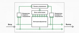
As a basic option, we propose the option of constructing a system of static voltage converters, shown in Fig. 1.
Rice. 1. Sketch of the functional diagram of single-phase and three-phase static voltage converters (SPO and SPT)
The proposed option logically follows from understanding the technical requirements of the task. Let's look at this in more detail. It is necessary to develop a three-phase static voltage converter with a power of 30 kW and a single-phase power converter with a power of 8 kW. The stated task implies the possibility (or even the necessity) of parallel inclusion of some minimal element. If we find the approximate least common multiple, it will be 3.3 kW. That is, the proposed option corresponds to Fig. 1: three three-phase 10 kW units (each with three 3.3 kW subunits) and one single-phase 8 kW unit (consisting of three 3.3 kW subunits with excess power).
The above system allows the use of: deep internal unification; parallel connection of three-phase units (SPT) and single-phase channels (SPO); increasing and decreasing the power of static voltage converters.
Let's consider the above point by point.
- The unification lies in the fact that the SPT and SPO blocks can be assembled on one printed circuit board, with the same mounted elements, with minor changes in switching (mainly in the high-current part) and in the configuration.
- Parallel connection of SPT blocks and SPO channels is possible when using IGBT bipolar transistors with a positive saturation voltage coefficient as power switches. In addition, dynamic current equalization and phase balancing are assigned to the control system. 3. Due to the parallel connection of blocks and channels, the proposed structure for constructing static voltage converters implies the ability to easily increase and decrease the power of static voltage converters. This option is a system for constructing static voltage converters based on a unified base cell (UBC). It is a complete unit that performs the functions of an AC input voltage rectifier, a power factor corrector, a DC voltage stabilizer, a DC-AC voltage converter and an AC output voltage stabilizer (with the function of an output voltage waveform corrector). Another undeniable advantage of this solution is the ability to vary the power of BYU. Accordingly, it is possible to systematically build various families of static voltage converters, covering all functional and parametric series.
Menu
In all developed countries, over 60% of generated electricity passes through semiconductor converters, and therefore the level of converter technology has a significant impact on the energy sector as a whole. In Russia today, only 30% of generated electricity passes through semiconductor converters. Estimates show that increasing this value to the world level will save more energy than, for example, all nuclear energy provides.
An approximate structure of electricity consumption is shown in Fig. 1. About 60% of consumption falls on the electric drive, where the transition from an unregulated drive to a controlled one using semiconductor frequency converters allows saving on average more than 25% of electricity. In transport, an adjustable drive with energy recovery into the network during braking saves about 30% of energy; static reactive power compensators of power lines, etc., provide greater savings.
Rice. 1. Electricity consumption structure
The main active elements of the converter are power semiconductor devices, and the main semiconductor material for more than forty-five years has been monocrystalline silicon.
Conventionally, modern power silicon devices can be divided into two large groups. The first group of devices, currently used mainly for converting very high powers (from several megawatts and above), are powerful diodes and thyristors, as well as turn-off thyristors (ST) and their modifications. The technological foundations for the production of devices of this group were laid in 1960–70. Devices of the second group - field-effect and bipolar field-effect transistors (MOSFET and IGBT) - are, in fact, a power integrated circuit of hundreds of thousands of elementary device cells on a single chip, manufactured on the basis of modern microelectronic technologies.
In the range of very high powers (tens of megawatts and above), the dominant device is a powerful high-voltage thyristor. The semiconductor structure of the thyristor (Fig. 2) consists of four silicon layers of alternating conductivity type located one above the other. They form three pn
-transition;
the two outer ones - the emitters - are shifted in the conductive direction, and the central one - the collector - in the shut-off direction; it blocks the voltage applied to the device. To switch the device, a short current pulse is passed in the base-cathode circuit, accompanied by the injection of electrons into the p
-base.
Since, due to the large tangential resistance of the thin p
-base, the control electronic current density quickly decreases with distance from the base contact, switching of the device occurs in a narrow (hundreds of microns) region along the base-collector boundary and then slowly spreads over the entire area. This is why the thyristor cannot be turned off by a reverse current pulse in the control circuit; To turn it off, you have to interrupt the current in the power circuit for the time required for the recombination of the electron-hole plasma in the bases. This is the main disadvantage of the thyristor, due to which it was replaced by devices with full control in a relatively narrow region of very high powers, where such advantages of the thyristor as low residual voltage at high forward current density and high operating voltage, high overload capacity and relatively low cost are decisive.
Rice. 2. Powerful high-voltage thyristor (with a silicon diameter of 125 mm, operating current 5 kA, blocking voltage 6 kV)
The parameters of modern high-voltage thyristors are very high. Thus, a thyristor with a silicon structure with a diameter of 125 mm has an average operating current of more than 5 kA at an operating voltage of 6 kV. The main areas of application are heavy-duty converters in DC power lines, DC insertions between power systems, static reactive power compensators in AC power lines and other powerful devices. As an example in Fig. Figure 3 shows a 250 kV, 300 MW DC link between power systems in Japan; a more powerful insert (400 kV, 1400 MW), located near Vyborg, has been uninterruptedly transmitting energy to the power systems of Finland for almost twenty years. In Fig. Figure 4 shows a thyristor unit (235 kV, 800 A) developed for the power transmission line PT Ekibastuz-Center (1.5 million V, 6000 MW, 2500 km).
Rice. 3. Thyristor DC insert between power systems (voltage 250 kV, power 300 MW)
Rice. 4. Thyristor unit for power transmission lines PT Ekibastuz-Center (6000 MW, 1.5 MV, 2500 km). Operating voltage 235 kV, current 800 A
In the range of powers of units and tens of megawatts, the dominant device is the turn-off thyristor - 3T (Fig. 5). Cathode n+p
-the emitter of this device consists of several thousand stripes, the half-width of which is approximately equal to the width of the initial inclusion region (Fig. 5b). With this geometry, the switching pulse of the control current affects the entire switched-on region of the emitter strip, interrupting the injection of electrons and thereby turning off the device. In this case, it is absolutely necessary to ensure strict synchronization of turning off all emitter strips, since mismatch leads to current localization and destruction of the device. In modern ECs, this problem is solved by the so-called “hard” switch-off: the switch-off current pulse has an amplitude comparable to the power current and a rise time of a fraction of a microsecond. The design of a powerful low-inductance system for such a shutdown is shown in Fig. 5th century This design of the EC with an integrated control system is now the main one; it is called Integrated Gate Commutated Thyristor (IGCT). Currently, the most powerful in the world is the ABB company's EC on silicon with a diameter of 140 mm - switchable current 6000 A, operating voltage 6 kV.
Rice. 5. Turn-off thyristor (GTO). Blockable current up to 6 kA, blockable voltage up to 6 kV, silicon Ø 140 mm
In the range of powers below several megawatts and frequencies from tens of hertz to tens of kilohertz, where the bulk of electricity is consumed, the dominant device is the insulated gate bipolar transistor (IGBT). It is a power integrated circuit; its elementary cell consists of a high-voltage bipolar transistor, the control circuit of which includes a field-effect transistor. The characteristic cell size is 10–15 µm, and a standard chip with an area of ∼1 cm2 accommodates several hundred thousand parallel working cells. The design of the unit cell is shown in Fig. 6. It consists of high voltage p+N+N–p+
-bipolar transistor and
N+pN–
field-effect transistor with an inversion channel.
When a positive bias is applied to the polysilicon gate of the field-effect transistor,
the inverse
n
the p closes
the N+
source with
the N–
layer.
The electronic current flowing in this circuit is the control current of the p+N+N–p+
bipolar transistor through which the power current flows. To turn off, a negative bias is applied to the gate, which leads to the rapid disappearance of the inverse channel and a break in the base current of the bipolar transistor, which comes out of saturation and turns off. The fundamental advantages of IGBTs are low power consumption in the control circuit for switching on and off, as well as high speed. The disadvantages are increased (compared to 3D) residual voltage in the on state, the complexity of assembling chips into a housing, as well as the high complexity of the manufacturing technology of the chips themselves.
Rice. 6. Insulated gate bipolar transistor (IGBT)
The current level of microelectronic technology makes it possible to produce IGBT chips with an area of ∼1 cm2 with an acceptable yield; the operating current of such a chip is ∼50–70 A. Parallel connection of chips is quite simple, and therefore IGBT modules for currents up to several kiloamperes are generally ordinary products.
The most popular sector of the global power electronics market—converters in the voltage range of 0.6–1.7 kV—is now entirely based on IGBTs. The next voltage range - up to 3.3 kV - is currently being intensively developed by leading companies. In the voltage range of 4.5–6.5 kV, typical for megawatt systems, IGBTs are still inferior to turn-off thyristors.
Low-power converters today are based mainly on high-power field-effect transistors (MOSFETs). Such a transistor is also a power integrated circuit consisting of hundreds of thousands of transistor cells. The operating voltage of high-power DCs usually does not exceed 500 V; the operating current is from units to hundreds of amperes, and the frequency range is up to hundreds of megahertz.
In the USSR, power semiconductor instrumentation as a branch of the electrical industry was created in the 1960–70s as a result of the joint work of the Physicotechnical Institute. Ioffe RAS, (Saransk) and VEI named after. Lenin (Moscow). The main devices of that time - power diodes and thyristors - were comparable in parameters to world standards, their cost - largely due to effective technology - was approximately three times lower than the world market, and the production volume at five specialized factories fully met the needs of all industries. In the mid-1970s, the industry began to lag behind the world level, which became catastrophic in the 1990s, when revolutionary changes occurred in world power electronics associated with the start of mass production of high-power field-effect and bipolar field-effect transistors. Due to known circumstances, Russian industry could not take any part in this process. As a result, Russia currently does not have its own production of the most popular power electronics devices. In 2004, the structure of the Russian market for power semiconductor devices with a total volume of about 2 billion rubles. looked like this: devices of the 1st group (thyristors and diodes) - 44% (own production and export), devices of the 2nd group (IGBT, MOSFET) - 56% (import only). Thus, Russia now spends more than a billion rubles annually on imports, mainly IGBTs, and, according to forecasts, in 2012 it will spend more than 6 billion rubles. Such dependence on imports is dangerous not only economically, but also strategically.
Generally speaking, small-scale IGBT assembly production based on imported chips already exists in Russia. Attempts were also made to create our own production of chips for the voltage range of 600–1700 V for the most widespread converter devices, but competition in this range from foreign companies turned out to be too high, and the following voltage ranges were up to 3 kV and 4.5–6.5 kV - too technically complex. Now at the Physicotechnical Institute. Ioffe, together with JSC Svetlana-Semiconductors, are working to create a device alternative to IGBT and designed for the range of 2.5–6.5 kV. The device is a microthyristor chip controlled by one external field-effect transistor with low channel resistance. This separation of the bipolar and field components greatly simplifies the technology and at the same time makes it possible to obtain static characteristics that are significantly better than those of IGBTs. The work is in its early stages, but the first results are encouraging. The design of the unit cell and microthyristor chip is shown in Fig. 7.
Rice. 9. Dynistor with fast ionization (FID) a) the process of forming ionization fronts at the collector of the dinistor structure and filling the base layers with plasma b) pulse generator for gas lasers (voltage 15 kV, current 1 kA, front 3 ns, frequency 100 Hz) c) pulse generator for powerful EM emitters (voltage 40 kV, peak power 70 MW, edge 140 ps, frequency 100 Hz)
The same processes occur in more complex thyristor structures. In Fig. Figure 9a shows the process of formation of ionization fronts at the collector of the dinistor structure and filling the base layers with plasma. After subnanosecond switching, the dinistor is maintained in the on state by a conventional thyristor mechanism. This device, called a fast ionization dynamistor (FID), is now the most efficient nano- and subnanosecond switch, on the basis of which powerful pulse generators for many branches of science and technology are produced and exported to almost all developed countries. In Fig. Figure 9b shows a typical generator for powering a nitrogen laser, and below is a powerful subnanosecond pulse generator with a peak power of 70 MW. On the basis of such generators, the Institute of Thermophysics of Extreme States, for example, built. phased arrays of ultra-powerful electromagnetic emitters with a peak power of the order of hundreds of megawatts or more. Such systems today can only be created in Russia, since only here there is the appropriate element base.
Recent numerical simulations have shown that, under certain conditions, a new type of front can be formed with a much higher travel speed than a conventional shock-ionization front. It turned out that if a reverse-biased silicon diode without deep centers in n
apply an even more rapidly (∼10 kV/ns) increasing overvoltage pulse to the base, then impact ionization does not develop until the field strength at the
pn
junction exceeds the tunnel ionization threshold (∼106 V/cm). The free electrons that appear after this find themselves in the region of a superstrong field and initiate an intense impact-ionization process, accompanied by the appearance of a high-concentration electron-hole plasma and the movement of a tunnel-impact-ionization front at a speed an order of magnitude greater than that of conventional impact-ionization fronts. As can be seen from Fig. 10, a switch created on the basis of this phenomenon must have unique characteristics: a silicon diode with a base thickness of 100 μm and an area of 2⋅10–3 cm2 generates a current pulse of 200 A in the load with a voltage of 8 kV and a rise time of 20 ps, and the speed The movement of the ionization front at the end of the process is only an order of magnitude less than the speed of light.
Rice. 11. Nanosecond generators based on SOS diodes a) voltage 1 MV, current 1 kA, duration 30 ns, frequency 300 Hz; b) voltage 400 kV, current 1.5 kA, duration 30 ns, frequency 300 Hz
As an example in Fig. Figure 11 shows two powerful SOS generators produced at the Institute of Experimental Physics, Ural Branch of the Russian Academy of Sciences; pulse power is more than a gigawatt at a voltage of 1 MV.
Microsecond switching of very large, hundreds of thousands and even millions of amperes, currents with semiconductor devices became possible after the creation at the Physicotechnical Institute of the Russian Academy of Sciences of a reversible dinistor, RVD. This is a thyristor-type device, the semiconductor structure of which consists of several tens of thousands of alternating thyristor and transistor sections with a common collector (Fig. 12a). To turn on the device, the polarity of the external voltage is changed for a short time (fractions of a microsecond), and a short current pulse passes through the transistor sections. Electron-hole plasma is injected into n
-base, creating a thin plasma layer over the entire collector plane.
The saturable reactor L separates the power and control circuits during this time. After a fraction of a microsecond, the reactor is saturated and a voltage of the original polarity is applied to the device. The external field pulls holes from the plasma layer into the p
-base, causing the injection of electrons
the n+
-emitter and switching the device uniformly and simultaneously over the entire area, almost regardless of its size. This nature of switching allows switching very large currents with a high rate of rise. A typical switching waveform is shown in Fig. 12b: A RVD with a silicon diameter of 76 mm, after passing a pump pulse, switches a current of 200 kA with a rise rate of 50 kA/μs. In principle, an RVD on a currently available silicon diameter of 140 mm will switch a current of about 1 million A. The limiting process is thermal lacing: when the concentration of thermally generated carriers approaches the concentration of the injected plasma, localization of the current occurs and destruction of the device. Typical designs of RVD keys are shown in Fig. 12v, g.
Rice. 13. Silicon carbide, SiC a) bulk SiC crystals (sublimation growth method) b) SiC wafer polished on both sides
In the 1980s, the USSR was a leader in the field of SiC technologies, but then, due to well-known events, funding for this work ceased, and the created technologies went abroad along with emigrants. In the USA, with broad government support, a very rapid development of SiC technologies began, which now continues at an increasing pace. And if decisive measures are not taken today, our lag will soon become hopeless. Until recently, this course of events seemed inevitable, but now there are some hopes. In the Republic of Mordovia, where a large plant is located that produces about 80% of Russian power semiconductor devices, work has begun on creating a SiC industry. Funds were allocated from the republican budget for the organization of the Research and Production Complex of Wide-Area Materials with a branch in St. Petersburg.
Within several years, it is planned to organize a small production with a full cycle: SiC monocrystals, wafers, epi-films and devices based on them.
MEAN WELL has released two new series of AC/DC converters: AS-120P (120 W adapter) and ASP-150 (150 W switching power supply in an open design, which differs from the AS-120P series sources in the absence of a plastic case). These series are characterized by low power consumption without load and an active power correction function. Thanks to modern ZCS/ZVS technology, these series sources have an efficiency of more than 90% and can provide a power of 120/150 W even with convection cooling.
The AS-120P Series is equipped with a standard 3-pole input and can be configured with input and output connectors to suit the end user's specifications (additional charges may only apply if custom connectors are ordered). With protection against short circuit, overload, overvoltage, overheating and a sealed housing, the AS-120P is suitable for powering LCD TVs and monitors, laptops, etc. The ASP-150 series is mainly designed for industrial use. Thanks to the low profile of 28.5 mm, the sources of this series can be successfully used in limited space and installed in 1U slots.
Main technical characteristics:
- universal entrance;
- power correction function;
- protection: short circuit, overload, overvoltage, overheating;
- convection cooling;
- ZCS/ZVS technologies to reduce energy dissipation;
- high specific density: 5 W/in3 (AS-120P); 8.8 W/in3 (ASP-150);
- no-load consumption <0.75 W at 240 V (< 1 W for ASP-150);
- Dimensions (WxHxD): 167x67x35mm (AS-120P), 169x60.7x28.5mm (ASP-150).
A set of control algorithms for a static voltage converter
The proposed set of control algorithms fully confirms the fulfillment of functional requirements. The first link control algorithm, based on a proportional position controller, is shown in Fig. 5.
Rice. 5. Control algorithm based on a positional proportional controller
The algorithm for dynamic control of the output current (Fig. 6) reveals additional functionality:
- dynamic equalization of output current when connected in parallel;
- dynamic regulation of the output current during non-emergency changes.
Rice. 6. Algorithm for dynamic control of output current
The basis is a superposition of two possible options for dynamic changes in the output current: by changing either the value of the intermediate constant voltage or the control coefficient kр. The functional algorithm for regulating the output current by changing the value of the intermediate DC voltage, prepared under the Capture shell, is presented in Fig. 7a.
Rice. 7. Functional algorithm for regulating the output current by changing
The functional algorithm for regulating the output current by changing the control coefficient kр, prepared under the Capture shell, is presented in Fig. 7b.
On
shows a dynamic increase in the output current from 37 to 48 A when the intermediate DC voltage changes from 350 to 450 V.
On
it is shown how a change in the control coefficient kр from 0.4 to 0.9 leads to an increase in the output current from 19 to 41 A.
The control algorithm for the second link based on a self-tuning system, based on sinusoidal pulse-width modulation, is shown in Fig. 10. This algorithm uses the method of stabilizing the output voltage (with the function of correcting the shape of the output voltage), when for each sampling point of the period the output voltage at this point is measured. Using the output voltage data, you can calculate the duration of the PWM signal for the next time slice.
Rice. 10. Control algorithm for a self-tuning system based on sinusoidal pulse width modulation
Description of the operation of a complex of control algorithms in the output voltage shape correction mode
Let's consider the operation of the presented circuit on a capacitive rectifier (
). This type of operation of static voltage converters occurs quite often. But most importantly, this option is characterized by maximum distortion of the output signal shape. Thus, this is the most visual representation of the algorithm’s capabilities in terms of correcting the output voltage shape.
Uncorrected output voltage of the circuit when operating on a capacitive rectifier (Fig. 12).
Rice. 12. Diagrams of the output voltage, PWM signal voltage and output current of the circuit when working on a capacitive rectifier
The figure shows that, despite the correct shape of the PWM signal, the shape of the output low-frequency signal is distorted. This makes it possible to construct a concept for correcting the output voltage waveform based on a change in the PWM signal proportional to the difference between the real signal and the ideal one. The control algorithm uses the method of stabilizing the output voltage (with the function of the output voltage shape corrector), when for each sampling point of the period the output voltage at this point is measured [3].
The presented results prove the viability of the proposed methods.
Using a set of control algorithms to prevent saturation of the output power transformer
The presented set of algorithms helps prevent saturation of the output power transformer core. Indeed, the core is designed so as not to enter the saturation region at the rated value of the output voltage with a margin necessary not only to correct the shape of the output voltage, but also to prevent emergency situations caused by various factors, for example, technological variations in the properties of materials.
As an example, consider the frequently encountered circuit of a bridge voltage inverter with an output power transformer, shown in
.
The control system modeled under the Capture shell in OrCAD 9.2 generates the output voltage shown in Fig. 14, via the PWM signal shown in Fig. 15.
Fig. 14. Output voltage of the simulated circuit
Rice. 15. PWM control signal of the simulated circuit
These figures illustrate the operation of the circuit under uniquely specified conditions. In real conditions, there are many destabilizing factors, so the inverter operating algorithm is aimed at compensating for their influence. However, it should be remembered: within the framework of the main operating algorithm, there is a possibility of reaching saturation of the power transformer (Fig. 16), which can lead to emergency consequences.
Rice. 16. Magnetization curve of the magnetic core of a power transformer
By supplementing the main operating algorithm with a simple protective algorithm (Fig. 17) and using insignificant free resources of the control system, we can avoid undesirable consequences.
Rice. 17. Control algorithm to prevent saturation of the output power transformer
The operating logic of the presented algorithm is based on the principle of self-preservation and provides for the termination of the execution of the main functional section of the algorithm (in this case, possibly correction of the output voltage shape) in order to prevent failure of the entire system. But the additional algorithm does not turn off the system, but somewhat reduces the quality of the output signal to maintain its functionality. In other words, one of the principles inherent in the intellect is used here - the principle of self-preservation.
In reality, this means that when a critical event occurs, the control system stops adjusting the shape of the output voltage and keeps the operation of the static voltage converter in the boundary state, despite distortions in the shape of the output voltage. The case under consideration prevents emergency failure of the output switches and is maintained until the operating conditions of the system change.
Active harmonic filters
Active harmonic filters (AHFs) are designed to provide a sinusoidal shape of the current consumed from the primary source under a nonlinear load [3, 7]. Such a load can be a converter with an uncontrolled or controlled rectifier. AFG analyzes the harmonic composition of the current at the input of the converter and generates higher harmonics of the current at the point of its connection in antiphase with the higher harmonics of the input current of the converter. As a result, higher harmonics are compensated (neutralized) and the current in the common circuit (consumed from the source) maintains a sinusoidal shape (Fig. 3). The configuration of the AFG power circuit is similar to a PWM rectifier, but its control algorithm is different. This is determined by the need to generate only high-frequency current components to compensate for reactive power and current distortion power in a nonlinear circuit.
Fig. 3 Block diagram of the DPE system with AFGB.
Figure 4 shows a diagram of the power stage of one arm of a three-phase AFG, which has a connection from the midpoint of the capacitive circuit C2, C3 to the neutral wire of the source. This structure makes it possible to compensate for higher current harmonics in an asymmetrical three-phase system. IGBT transistors are controlled according to a specific algorithm as a result of monitoring load currents and compensation circuits. Current analysis occurs with a discreteness of 256 measurements per fundamental harmonic period [10]. Calculations are performed by the DSP controller during each period and then the generated correction signal affects the PWM control system of the inverter transistors. Thus, the control process occurs with a delay of one period of the fundamental frequency, which can create problems in dynamic modes.
Fig.4 Power circuit of one arm of the AFG 1. Higher harmonic recognition unit, 2. Control signal generation unit, 3. IGBT transistor driver.
A feature of the AFG is that it is not required to produce active power to compensate for higher harmonics. The DC link capacitance and input filter inductance values are selected based on the existing reactive power and harmonic distortion power that must be compensated. The AFG input filter contains a relatively large inductance L1 to convert the voltage at the inverter output into a current sequence to compensate for higher harmonics. Capacitance C1 and inductance L2 are designed to smooth out ripples at high frequencies. The desired shape of the current is obtained due to a certain control law of the IGBTs - the inverter transistors. The higher the order of the current harmonic being compensated, the higher the value should be. The higher the value of inductance L1, the better the isolation from the primary source of the AFG power circuit and the better the protection from transient disturbances, but the more difficult it is to ensure high values. Thus, the inductance of the input filter limits the ability of the AFG to compensate for higher order harmonics.
AFG is an adaptive device for suppressing higher harmonics, also called an active harmonic conditioner [33].
Issues of control strategy, AFG topology, selection of current range, switching frequency of power transistors, etc. a significant number of publications are devoted [7, 10, 29, 33-39]. However, the influence of the inductance values of the input filter and capacitance in the power structure of the AFG on the static and dynamic characteristics of the system has not been studied. The issues of the optimal control algorithm for power transistors AFG, etc. remain unresolved.
Selection of element base, design features of a unified cell and brief analysis
The most critical elements of our circuit are the power switches. This is caused by our chosen conversion frequency of 40 kHz.
Based on this, we choose IGBT bipolar transistors Power MOS 7 from Advanced Power Technology [1].
As our experience in the field of microelectronics shows, the presented technological features effectively act in the indicated directions, which confirms the by no means declarative nature of the declared electrical parameters.
The information provided indicates full compliance of the parameters of IGBT bipolar transistors with the requirements for them in the developed circuit.
The selected algorithms and parameters of the control system, as well as the functional tasks assigned to the system, force us to use a controller with a digital signal processor in the control system. From the point of view of the tasks set, namely, controlling the shape of the output voltage for each PWM quantum, measuring the current of each switch in order to dynamically equalize the currents of parallel-connected subblocks and operating IGBT bipolar transistors at a frequency of 40 kHz, DSPs have an overwhelming advantage.
The most commonly used digital signal processors in secondary power supply control systems are the TMS320 series from Texas Instrument. The TMS320 series DSPs are characterized by high performance and a large number of peripheral devices, which are essential when building control systems for static voltage converters.
However, recently microprocessors with similar characteristics, but cheaper to operate, have appeared.
The cell dimensions are determined by the restrictions imposed on the dimensions in plan (600×600 mm) and height (600 mm).
That is, if the cell fits into the size 19″×19″ = (482.6×482.6 mm), we will fulfill the first requirement and the requirements of international unification. Based on the second requirement and the overall dimensions of the power elements, the cell height should not exceed 150 mm.
The selected circuit solutions and element base allow us to fit into the specified dimensions.
Structurally, the cell is built in a classic way: on the front panel there is a discrete input/output board, a microcontroller and signal switching elements; at the rear there is a radiator with powerful heat-generating elements and powerful switching elements; between them is a board with the rest of the circuit elements. This arrangement, as practice shows, helps solve thermal problems. In addition, modeling electromagnetic processes at the design development stage will allow solving many issues of electromagnetic compatibility. After modeling, SEMIKRON reduced the level of spurious electromagnetic radiation in its smart modules by 2 times [6].
Now let's look at specific power - one of the indicators of modern power electronics voltage converters, which clearly characterizes the quality of the product. The maximum permissible power of our voltage converter is 4000 W. The volume of the block is 4.826×4.826×1.5 = 34.94 dm3. The specific power of our two-stage multifunctional voltage converter is 4000/34.94 = 114.5 (W/dm3), which is quite good by modern standards even for a single-stage voltage converter. In addition, it is possible to double the power while maintaining the same dimensions.
Having examined the results obtained, it can be argued that the developed preliminary design is the basis of a family of static voltage converters of a new generation. This solution not only meets the objectives, but also allows you to significantly expand the area of its use.
Generalization of the results obtained and methods used
The presented option is one of many possible ones. But I would like to highlight some patterns identified during the work and make generalizations:
- Digital, in particular microprocessor-based devices, are becoming increasingly common in control systems of both general and power electronics.
- This allows you to create a number of functionally diverse devices using uniform, optimal circuitry.
- The variety of functions and parameters performed is increasingly determined by the algorithms and software used.
- Algorithmization of control allows not only to achieve new functionality, but also to make the control process visual, logical, simple and reliable.
- The proposed technique is in line with the development of electronics in general.
In conclusion, I would like to note that the considered methodology can be extended not only to other types of power supplies, but also to other types of power electronics, in particular, to drive control.
Literature
- Shchukina I., Nekrasov M. New technology PT IGBT against powerful field-effect transistors // Power Electronics. 2004. No. 1.
- Single-stage power factor corrector // Circuitry. 2001. No. 10.
- Temirev A.P., Fedorov A.E., Masnyuk S.I., Yurin A.V. Algorithm for generating sinusoidal voltage for uninterruptible power supply systems // Power supply. 2003. Vol. 5.
- Silkin V. A. Option for constructing static voltage converters // Components and Technologies. 2004. No. 8.
- Silkin V. A. An example of creating a complex of control algorithms for high-quality static voltage converters // Components and Technologies. 2004. No. 9.
- Silkin V. A. Optimization of electromagnetic compatibility based on 3D mapping and classical theory of circuits with distributed parameters // Components and Technologies. 2005. No. 2.
- Silkin V. A. “Intellectualization” of electronic devices // Components and Technologies. 2005. No. 3.
- Silkin V. A. Draft design of a system of static voltage converters // Modern electronics. 2005. No. 3.
Literature
- Klimov V.P. Uninterruptible power supplies of the DPK series of medium power, Electric Power, No. 2, 2006.
- V. Klimov, A. Moskalev Three-phase uninterruptible power supplies: circuit design and technical characteristics, Electronic components, No. 8, 2005.
- Klimov V.P., Moskalev A.D. Methods for suppressing harmonics in power supply systems, Practical Power Electronics, No. 6, 2003.
- Development and production of power electronics, Catalog of products and applications, Triol Corporation, 2002.
- V. Klimov, S. Klimova Energy performance of uninterruptible AC power supplies, Electronic components, No. 4, 2004.
- Vorobiev A.Yu. The influence of UPS on the power supply system, Communications Bulletin, No. 7, 2006.
- Agunov A.V. Static compensator of inactive power components with full compensation of harmonic components of the load current, Electrical Engineering, No. 2, 2003.
- I.M. Chizhenko, V.S. Rudenko, V.I. Senko Fundamentals of converter technology, M., Higher School, 1974.
- PW Wheeler et al. Electromechanical drive with a matrix-type converter and an electric machine with permanent magnets in an aircraft rudder drive, Power Electronics, No. 4, 2006.
- Mark McGranagham Active Filter Design and Specification for Control of Harmonics in Industrial and Commercial Facilities, Electrotek Concepts, Inc. Knoxville TN, USA, 2000.
- JW Dixon, JM Contardo, LA Moran A Fuzzy-controlled Active Front-end Rectifier with Current Harmonic Filtering Characteristics and Minimum Sensing Variables, IEEE Trans. On Power Electronics, vol.14, no.4, 1999.
- T. Kataoka, Y. Fuse, D. Nakajima, S. Nishikata A three-phases Voltage-type PWM Rectifier with the Function of an Active Power Filter, Proc. Power Electronics and Variable Speed Drives, 2000.
- T. Tomas, K. Haddad, G. Joos, A. Jaafari Design and Performance of Active Power filters, IEEE Industry Application Magazine, vol.4, no.5, 1998.
- W. McGrady, M. J. Samotryi, A. H. Noyola Survey of Active Power Line Conditioning Methodologies, IEEE Trans. On Power Delivery, vol.5, 1990.
- S. Kwak, H. A. Toliyat A matrix Converter for Fault Tolerant Strategies and two-phases Machine Drives, Proc. IEEE IECON'02, vol.1, 2002.
- R. Ribeiro, C. Jacobina, E. Silva, A. Lima Fault-tolerant Voltage-fed PWM Inverter AC Motor Drive Systems, IEEE Trans. on Industry Applications, vol.51, no.2, 2004.
- A. Alesina, M. Venturini Analysis and Design of Optimum-amplitude Nine-switch Direct AC-AC Converters, IEEE Trans. on Power Electronics, vol.4, no.1, 1989.
- L. Zhang, C. Watthanasarn, W. Shepherd Control of AC-AC Matrix Converters for Unbalanced and/or Destored Supply Voltage, Proc. IEEE PESC'01, vol.2, 2001.
- Casadei D., Serra G., Tani A., Zarri L. Matrix Converter Modulation Strategies: A New General Approach Based on Space-Vector Representation of the Switch State, IEEE Trans. on Power Electronics, vol.49, no.2, 2002.
- Wheeler P.W., Rodriguer J., Clare J.C., Empringham L., Weinstein A. Matrix Converters: A Technology Review, IEEE Trans. on Industrial Electronics, vol.49, no.2, 2002.
- L. Huber, D. Borojevic Space Vector Modulated Three-phases to Three-phases Matrix Converter with Input Power Factor Correction, IEEE Trans. on Industry Applications, vol.31, no.6, 1995.
- O. Simon, J. Mahlein, M,N. Muenzer, M. Bruckmann Modern Solutions for Industrial Matrix-Converter Applications, IEEE Trans. on Industrial Electronics. Vol.49, no.2, 2002.
- J. R. Fu, T. A. Lipo Disturbance-free Operation of a Multiphase Current-regulated Motor Drive with an Open Phase, IEEE Trans. on Industry Applications, vol.3, no.5, 1994.
- S. Bolognani, M. Zordan, M. Zigliotto Experimental Fault-tolerant Control of a PMSM Drive, IEEE Trans. on Industrial Electronics, vol.47, no.5, 2000.
- Tian-Hua Liu, Che-Kai Hung, Der-Fa Chen A Matrix Converter - Fed Sensorless PMSM Drive System, Electric Power Components and Systems, vol.33, no.8, 2005.
- S. Bernet, S. Ponnaluri, R. Teichmann Design and Loss Comparison of Matrix Converters and Voltage-source Converters for Modern AC Drives, IEEE Trans. on Industrial Electronics, vol.49, no.2, 2002.
- Kyo-Beum Lee, Frede Blaabjerg Reduced Order Extended Luenberger Observer Based Sensorless Vector Control Driven by Matrix Converter with Non-linearity Compensation, IEEE Trans. on Industrial Electronics, vol.53, no.1, 2006.
- A. Arias, C. A. Silva, G. M. Asher, J. C. Clare, P. W. Wheeler Use of a Matrix Converter to Enhance the Sensorless Control of a Surface Mount Permanent Magnet AC Motor at Zero and Low frequency, IEEE Trans. on Industrial Electronics, vol.53, no.2, 2006.
- S. Bhattacharya, T. M. Frank, D. M. Divan, B. Banerjee Active Filter System Implementation, IEEE Industry Applications Magazine, vol.4, no.5, 1998.
- A. M. Trzynadlowski, N. Patriciu, F. Blaabjerg, J. K. Pederson A Hybrid, Current-source/Voltage-source Power Inverter Circuit, IEEE Trans. on Power Electronics, vol.16, no.6, 2001.
- F. Blaabjerg, U. Jaeger, S. M. Nielsen, J. K. Pederson Power Losses in PWM-VSI Inverter Using NPT or PT IGBT Devices, IEEE Trans. on Power Electronics, vol.10, no.3, 1995.
- S.Kwak, H. A. Toliyat A Hybrid Converter System for High Performance Large Induction Motor Drives, IEEE Proc. APEC'04, vol.1, 2004.
- R. M. Duke, S. D. Round The Steady-state Performance of a Controlled Current Active Filter, IEEE Trans. on Power Electronics, vol.8, no.3, 1993.
- VB Bhavaraju, Pn Enjeti Analysis and Design of an Active Power Filter for Balancing Unbalanced Loads, vol.8, no.4, 1993.
- Fang-Zhang Peng, H. Akagi, A. Nabae A Study of Active Power Filters Using Quad-series Voltage Source PWM Converters for Harmonic Compensation, IEEE Trans. on Power Electronics, vol.5, no.1, 1990.
- S. Bernard, G. Trochain Second Generation of High Power Active Harmonic Conditioner Based on the Current Injection Principle, MGE UPS Systems, MGE0121UKI-98, 1998.
- S. Bernard, G. Trochain Compensation of Harmonic Currents Generated by Computers Utilizing an Innovative Active Harmonic Conditioner, MGE UPS Systems, MGE0128UKI-2000, 2000.
- G. W. Massey Power Distribution System Design for Operation under Nonsinusoidal Load Conditions, IEEE Trans. on Industry Applications, vol.31, no.3, 1995.
- S. Fukuda, T. Endoh Control Method for a Combined Active Filter System Employing a Current Source Converter, IEEE Trans. on Industry Applications, vol.31, no.3, 1995.
- Switch Mode Inverter. The Smart AC Power Solution, CE+T, www.cet.be
- Multi DIALOG MDT & MDT-AF, www.advancedpower.co.uk