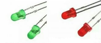
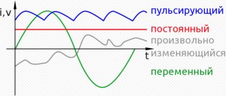
LEDs are used in almost all technology around us. True, sometimes it becomes necessary to adjust their brightness (for example, in flashlights or monitors). The easiest way out in this situation seems to be to change the amount of current passed through the LED. But that's not true. The LED is a fairly sensitive component. Constantly changing the amount of current can significantly shorten its life, or even break it. It is also necessary to take into account that you cannot use a limiting resistor, since excess energy will accumulate in it. This is unacceptable when using batteries. Another problem with this approach is that the color of the light will change.
PWM regulation
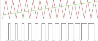
A way out of this situation may be to use pulse width modulation (PWM). With this system, the LEDs receive the required current, and the brightness is adjusted using high-frequency power supply. That is, the frequency of the feeding period changes the brightness of the LEDs. The undoubted advantage of the PWM system is maintaining the productivity of the LED. The efficiency will be about 90%.
Introduction
The exponential growth of LED lighting is accompanied by an expanding selection of chips for driving LEDs. Switching LED drivers have long replaced linear current sources, which consume significantly more energy. All applications, from flashlights to stadium scoreboards, require precise control of regulated current. In many cases, it is necessary to change the output intensity of LEDs in real time. This function is commonly referred to as LED dimming. This article introduces the basic concepts of LED theory as well as some brightness control techniques for switching LED drivers.
PWM generators
In a PWM system, a microcontroller or a circuit consisting of low-integration circuits can be used as a master oscillator. It is also possible to create a regulator from microcircuits that are designed for switching power supplies, or K561 logic chips, or NE565 integrated timer. Craftsmen even use an operational amplifier for these purposes. To do this, a generator is assembled on it, which can be adjusted. One of the most used circuits is based on the 555 timer. It is essentially a regular square wave generator. The frequency is regulated by capacitor C1. at the output the capacitor must have a high voltage (this is the same with the connection to the positive power supply). And it charges when there is a low voltage at the output. This moment gives rise to pulses of different widths. Another popular circuit is PWM based on the UC3843 chip. in this case, the switching circuit has been changed towards simplification. In order to control the pulse width, a control voltage of positive polarity is used. In this case, the output produces the desired PWM pulse signal. The regulating voltage acts on the output as follows: as it decreases, the width increases.
Add a link to a discussion of the article on the forum
RadioKot >Laboratory >Digital devices >
| Article tags: | Add a tag |
Remaking the TV backlight (eliminating PWM flicker)
Author: SSMix Published 09/23/2019 Created using KotoEd. Participant of the Competition “Congratulate the Cat as a Human 2022!”
The article describes a simple procedure for remaking the LG 32LN570V TV in terms of eliminating PWM ripples in the screen backlight.
In modern LCD TVs with LED backlighting, there is such a typical unpleasant malfunction as the burnout of one of the LEDs of this very backlight. Visually, this is manifested in the absence of a glow on the screen (although the backlight may periodically appear briefly after switching on at a very low brightness). If you shine an external light source on the screen, you can see some image. The sound is present. The thing is that several dozen powerful backlight LEDs are connected in series, like in a garland, and the burnout of one of them leads to an increase in the supply voltage of the LED chain by the control circuit in an attempt to stabilize the given backlight current. The LG 32LN570V TV model has 21 LATWT470RELZK LEDs in the backlight, 1 W each. During normal operation, the voltage on the chain of LEDs drops to about 75...80 V. If one of the LEDs breaks, the voltage increases to 135 V and the protection is triggered. In this case, short-term periodic illumination of the screen may occur when a small current flows through a faulty LED. Repairing such a malfunction in backlit TVs is not a pleasant pleasure. To get to the LED bars, you need to disassemble the matrix completely - with all the filters, polarizing and other films. In this case, there is a risk of damaging the matrix itself mechanically by inadvertently peeling off the glued cables from it. After repairing the backlight, you need to put everything back in the same sequence. Videos on the backlight repair procedure for this TV model can be found on Youtube. An interesting video was also found there: “Converting an LED monitor to Flicker-Free technology (no flicker)”, in which the author uses a filter and an external powerful transistor, which dissipates excess backlight power. This article will talk about how adjusting the backlight current works, how to prevent such a malfunction from occurring and remove PWM backlight flicker in a more economical way. Physically, the backlight control circuit is located in the TV power supply:
Here is a fragment of the electrical backlight control circuit:
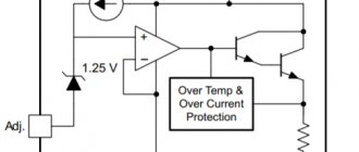
The specialized microcircuit IC801 MAP3202SIRH includes: - a boost converter controller (Q801, Q803, L801, D801, C801) with a built-in oscillator and feedback for voltage (R831, R830, R813) and current (R820), - a key transistor control circuit Q802 with current feedback (R822...R829), - internal 5V reference voltage source with load current up to 10 mA, PWM modulation circuit (PWMI input), - protection circuits: - from low supply voltage (<8V), - from increased current of the boost converter (>0.36V at the CS input), - from exceeding the supply voltage of the LED chain (>3V at the OVP pin), - from exceeding the backlight current (at the FBN pin). Here is a typical MAP3202 connection diagram:
Vin is the input voltage of the boost converter, indicated on the power supply diagram as DD (+33V). A chain of voltage feedback resistors (R831, R830, R813) limits the output voltage to 135V. Resistors at the source of the key transistor Q802 (R822…R829) with a resulting resistance RLED = 2.05 Ohms determine the current through the backlight LEDs as ILED = VFBP / RLED. The reference voltage VFBP is set by the resistive divider R811, R814 and is VFBP=R814*UREF/(R811+R814)=10k*5V/(51k+10k)=0.81967V. Hence the maximum backlight current ILED=0.81967V/2.05 Ohm=400mA. If we assume that the voltage drop across one LATWT470RELZK LED is 3.05-3.65V, then in the worst case, at a current of 400 mA, it will dissipate a power of 3.65V*0.4A=1.46W. To reduce the maximum current through the LEDs, one chain of resistors R826, R827 was soldered, as a result of which the resulting RLED resistance became equal to 2.73V, and the maximum backlight current decreased to ILED=0.81967V/2.73 Ohm=300mA. The power dissipation of each LED has also been reduced to 1W. Subjectively, the brightness of the screen did not decrease too noticeably, the margin remained significant, so in principle you can leave only 2 pairs of current-setting resistors to increase the reliability of the LEDs. The backlight current adjustment in the TV model under consideration is performed by PWM modulation of the current through LEDs. The PWM frequency during operation is 120Hz (in the absence of a signal, the frequency can decrease to 100Hz). The duty cycle is adjusted from the BACKLIGHT menu, and also within small limits automatically depending on the subject of the image. A PWM signal with a swing of 3.3V and a frequency of 120 Hz is supplied to the PWMI pin of the MAP3202 chip. The PWMO output provides PWM control of the key transistor Q802. Moreover, PWM modulation is available at the PWMI input even when the backlight level is set to 100% from the menu. This is what the pulsation of the TV screen looks like (white field signal, backlight 100%, contrast 55%, brightness 50%):
For the experiment, the contact with the PWMI wire was removed from the P201 connector, and a 22k variable resistor was soldered parallel to the R804 10k resistor. PWM flicker has completely disappeared, and the backlight current can be adjusted using an additional variable resistor at the FBP pin of the MAP3202 chip, reducing the reference voltage at this pin. It would be possible to leave everything this way (the working, simplest and fastest option) by attaching an additional resistor inside the TV with the handle exposed through the back cover, but I wanted to retain the ability to quickly adjust the backlight level directly from the TV remote control. Moreover, in this model, its own settings are remembered for each signal source. For this purpose, a small circuit was developed that converts the PWM backlight control signal into a shunt resistor R804 resistance. In this case, under no circumstances should the voltage at the FBP input of the MAP3202 microcircuit exceed 0.81967V specified by the voltage divider R811, R814, so as not to damage the backlight LEDs with increased current. Here is the diagram:
The PWM signal of the backlight level with a swing of 3.3V is supplied to the limiter R1, DA1 to eliminate the influence of the swing of the control signal on the backlight current. The PWM signal, limited at 2.5 V, is divided by K = 3.12 times and smoothed by elements R2, R3, C1, after which it is fed to the non-inverting input of the op-amp DA2.1 MCP6002. From its output, the voltage is supplied to the second chain of the RC filter R4, C2 and the voltage follower to DA2.2. The repeater output through the limiting resistor R5 1k and the protective diode VD1 is supplied to the FBP input of the MAP3202 microcircuit of the TV power supply. The feedback voltage from the FBP is applied to the inverting input of the first op-amp. Thus, the input voltage at the non-inverting input of the first op-amp (i.e., at the output of the circuit) is maintained equal to the output voltage at the input of the FBP MAP3202. With a 100% backlight level set, the input voltage of the op-amp will be 2.5V/3.12=0.801V, i.e. will not exceed the standard level of +0.8196V at the FBP input. Diode VD1 prevents high voltage from reaching the FBP input in emergency situations. In fact, the circuit through the VD1 diode only bypasses the lower resistor R804 10k in the standard divider at the FBP input. Also, diode VD1 performs another important function. At the minimum backlight level, it prevents the voltage at the FBP input of the MAP3202 chip from decreasing to zero, otherwise the image on the screen becomes too dark. The additional circuit is assembled on a single-sided printed circuit board measuring 16x17mm:
The connection to the TV power supply board is made using 4 wires. Before rework:
After the rework:
The PWMI input is taken from jumper J3, which is desoldered, breaking the circuit to the PWMI MAP3202. Front view when assembled:
After the modification, the control voltage was measured at the input of the FBP MAP3202 and the currents through the backlight LEDs were calculated taking into account the resistance RLED = 2.733 Ohm:
| Backlight level | FBP MAP3202 input voltage, mV | Current through backlight LEDs, mA |
| 100% | 788 | 288 |
| 50% | 485 | 177 |
| 45% | 415 | 151 |
| 1% | 247 | 90 |
The additional scarf itself was wrapped in heat shrink and left hanging on 4 wires:
After the rework, the result was a complete absence of ripples throughout the entire range of adjustments (white field signal, backlight 45%, contrast 100%, brightness 50%):
Moreover, if before the rework, to reduce the effect of PWM flicker on vision, it was necessary to set the backlight level to 100%, reducing the excessive brightness of the screen by reducing the contrast (i.e., reducing the light transmission of the matrix), now the contrast can be set to 100%, and the backlight level can be adjusted and brightness. As you can see in the first photo, the brightness level of the screen before the alteration when brought close to the screen was 96 lux with a backlight current of 400mA (100% backlight level). After reworking at a current of 151mA, the brightness level was 81 lux at 45% backlight. Thus, the comfortable backlight current was reduced by 2.65 times, which had a beneficial effect on the thermal conditions of the LEDs and the durability of their operation, and PWM flickering of the screen backlight was completely eliminated. The heating of the back wall of the TV after modification has noticeably decreased. A similar modification can be made on other TV models that use the MAP3202 or similar chip.
Files:
Files for the article
All questions in the Forum.
| What do you think of this article? | Did this device work for you? | |
| 20 | 10 | 5 |
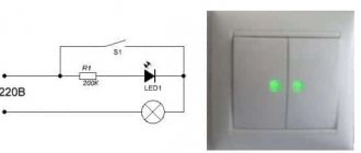
Why PWM?
- The main advantage of this system is its ease. The usage patterns are very simple and easy to implement.
- The PWM control system provides a very wide range of brightness adjustment. If we talk about monitors, it is possible to use CCFL backlight, but in this case the brightness can only be reduced by half, since CCFL backlight is very demanding on the amount of current and voltage.
- Using PWM, you can keep the current at a constant level, which means the LEDs will not be damaged and the color temperature will not change.
LED brightness and color temperature
LED brightness
The concept of brightness of visible light emitted by an LED is quite simple to explain. The numerical value of the perceived brightness of an LED can be easily measured in luminous flux density units called candelas (cd). The total output power of an LED is measured in lumens (lm).
It is also important to understand that the average forward current of an LED determines the brightness of the LED. Figure 1 shows the LED forward current as a function of light output. It can be seen from the figure that this dependence is linear over a wide range of applied values of the forward current IF. Note that as IF increases, the nonlinearity increases. When the current begins to go beyond the linear region, a decrease in efficiency (lm/W) occurs.
Rice. 1. Dependence of the light output on the LED current
Operating the LED in a mode exceeding the linear change range of the light output leads to the conversion of the LED output power into heat. This, in turn, creates a load on the LED driver and complicates the heat dissipation system.
LED color temperature
Color temperature is an indicator that describes the color of the LED and is indicated in the technical documentation for the LED. LED color temperature is defined over a range of values and varies with forward current, junction temperature, and LED life. Lower color temperatures correspond to red-yellow colors (which are called warm), and higher color temperatures correspond to blue-green colors (cool). Many color LEDs specify a predominant wavelength rather than a color temperature, and also allow wavelength shifts.
LM3409 provides multiple brightness adjustment functions
National Semiconductor's LM3409 is a unique LED driver that provides the necessary functionality for simple analog and PWM dimming. This device provides four possible ways to implement LED brightness adjustment:
- Analog adjustment using direct control of the IADJ pin from a voltage source in the range 0...1.24 V.
- Analog adjustment using a potentiometer connected between the IADJ pin and ground.
- PWM control using the resolution pin.
- PWM control using external shunt FETs.
The LM3409 circuitry for analog adjustment using a potentiometer is shown in Figure 6. An internal 5-µA current source creates a voltage drop across the RADJ, which in turn allows the internal current sensitivity threshold to be varied. For the same purpose, the IADJ pin can be directly driven from a constant voltage source.
Rice. 6. Connection diagram of LM3409 for analog brightness control.
Figure 7 shows a graph of the LED current versus the resistance of the potentiometer connected between the IADJ and GND pins. The flat part of the curve at a current value of 1 A corresponds to the maximum rated current of the LED, which is set by the current control resistor RSNS, shown in Figure 4.
Rice. 7. LED Current vs. Potentiometer Resistance
Figure 8 shows the LED current as a function of the voltage at the IADJ pin. Note that this graph shows the same maximum LED current set by the RSNS resistor.
Rice. 8. LED current versus voltage at the IADJ pin.
Both analogue control options are easy to implement and provide very linear levels of LED brightness reduction up to 10% of the maximum value.
Methods for adjusting LED brightness
There are two popular methods for adjusting the brightness of LEDs in switching driver circuits: PWM dimming and analog dimming. Both methods control time-averaged current through an LED or string of LEDs, but there are differences between them that become clear when discussing the advantages and disadvantages of the two types of control circuits.
Figure 2 shows a switching LED driver enabled in a buck topology. The VIN voltage should always be higher than the LED voltage plus the RSNS voltage. The current in the inductor is the LED current. Current stabilization occurs by monitoring the voltage at the CS pin. When the voltage at the CS pin begins to fall below the set voltage, the duty cycle of the current pulses flowing through the L1 coil, the LED, and the RSNS resistor increases, thereby increasing the average LED current.
Rice. 2. Buck regulator topology
IP calculation method based on the NCP1014 controller
Let's consider the method of step-by-step calculation of a flyback converter based on NCP1014 using the example of a reference design of a power supply with an output power of up to 5 W to power a system of three series-connected LEDs [3]. One-watt white LEDs with a normalization current of 350 mA and a voltage drop of 3.9 V are considered as LEDs.
The first step is to determine the input, output and power characteristics of the developed IP:
- input voltage range - Vac(min) = 85V, Vac(max) = 265V;
- output parameters - Vout = 3x3.9V ≈ 11.75V, Iout = 350mA;
- output power - Pout = VoutхIout = 11.75 Vх0.35 A ≈ 4.1 W
- input power - Pin = Pout/h, where h is estimated efficiency = 78%
Pin=4.1W/0.78=5.25W
- DC input voltage range
Vdc(min) = Vdc(min) x 1.41 = 85 x 1.41 = 120 V (dc)
Vdc(max) = Vdc(max) x 1.41 = 265 x 1.41 = 375 V (dc)
- average input current - Iin(avg) = Pin / Vdc(min) ≈ 5.25/120 ≈ 44mA
- peak input current - Ipeak = 5xIin(avg) ≈ 220 mA.
The first input link is the fuse and EMI filter, and their selection is the second step in power supply design. The fuse must be selected based on the breaking current value, and in the presented design, a fuse with a breaking current of 2 A is selected. We will not delve into the procedure for calculating the input filter, but only note that the degree of suppression of common-mode and differential noise largely depends on the topology of the printed circuit board , as well as the proximity of the filter to the power connector.
The third step is to calculate the parameters and select the diode bridge. The key parameters here are:
- permissible reverse (blocking) diode voltage - VR ≥ Vdc(max) = 375V;
- forward diode current - IF ≥ 1.5xIin(avg) = 1.5x0.044 = 66mA;
- permissible overload current (surge current), which can reach five times the average current:
IFSM ≥ 5 x IF = 5 x 0.066 = 330 mA.
The fourth step is to calculate the parameters of the input capacitor installed at the output of the diode bridge. The size of the input capacitor is determined by the peak value of the rectified input voltage and the specified level of input ripple. A larger input capacitor provides lower ripple values, but increases the inrush current of the power supply. In general, the capacitance of a capacitor is determined by the following formula:
Cin = Pin/, where
fac is the frequency of the AC mains (60 Hz for the design considered);
DV is the permissible ripple level (20% of Vdc(min) in our case).
Cin = 5.25/[60 x (1202 - 962)] = 17 µF.
In our case, we choose an aluminum electrolytic capacitor with a capacity of 33 μF.
The fifth and main step is the calculation of the winding product - a pulse transformer. The calculation of the transformer is the most complex, important and “subtle” part of the entire calculation of the power source. The main functions of the transformer in a flyback converter are the accumulation of energy when the control switch is closed and current flows through its primary winding, and then its transmission to the secondary winding when the power to the primary part of the circuit is turned off.
Taking into account the input and output characteristics of the power supply calculated in the first step, as well as the requirements for ensuring the operation of the power supply in the transformer continuous current mode, the maximum value of the duty cycle is 48%. We will carry out all calculations of the transformer based on this fill factor value. Let us summarize the calculated and specified values of the key parameters:
- controller operating frequency fop= 100 kHz
- fill factor dmax= 48%
- minimum input voltage Vin(min) = Vdc(min) - 20% = 96V
- output power Pout= 4.1W
- estimated efficiency valueh = 78%
- Peak value of input current Ipeak= 220mA
Now we can calculate the inductance of the primary winding of the transformer:
Lpri = Vin(min) x dmax/(Ipeak x fop) = 2.09 mH
The ratio of the number of turns of windings is determined by the equation:
Npri/Nsec = Vdc(min) x dmax/(Vout + VF x (1 - dmax)) ≈ 7
All we have to do is check the ability of the transformer to “pump” the required output power through itself. This can be done using the following equation:
Pin(core) = Lpri x I2peak x fop/2 ≥ Pout
Pin(core) = 2.09 mH x 0.222 x 100 kHz/2 = 5.05 W ≥ 4.1 W.
From the results it follows that our transformer can pump the required power.
It can be noted that here we have not given a complete calculation of the parameters of the transformer, but have only determined its inductive characteristics and shown the sufficient power of the chosen solution. Many works have been written on the calculation of transformers, and the reader can find calculation methods of interest, for example, in [4] or [5]. Coverage of these techniques is beyond the scope of this article.
The electrical circuit of the power supply, corresponding to the calculations performed, is presented in Figure 5.
Rice. 5. Schematic diagram of the IP
Now it’s time to get acquainted with the features of the above solution, the calculation of which was not given above, but which are of great importance for the functioning of our IP and understanding the features of the implementation of the protective mechanisms implemented by the NCP1014 controller.
Would you like to meet NCP1014 in person? - No problem!
For those who, before starting to develop their own IP based on NCP1014, want to make sure that this is a truly simple, reliable and effective solution, ONSemiconductor produces several types of evaluation boards (see Table 1, Fig. 6; available for order through COMPEL) .
Table 1. Overview of evaluation boards
| Order code | Name | Short description |
| NCP1014LEDGTGEVB | 8W LED driver with 0.8 power factor | The board is designed to demonstrate the possibility of building an LED driver with a power factor > 0.7 (Energy Star standard) without the use of an additional PFC chip. The 8 W output power makes this solution ideal for powering structures like the Cree XLAMP MC-E, which contain four LEDs in series in one package. |
| NCP1014STBUCGEVB | Non-inverting buck converter | The board is proof of the statement that the NCP1014 controller is sufficient to build low-price power supplies for harsh operating conditions. |
Rice. 6. Appearance of the evaluation board
In addition, there are several more examples of ready-made designs of various IPs, in addition to those discussed in the article. This is a 5 W AC/DC adapter for cell phones [6], and another IP option for LED [7], as well as a large number of articles on the use of the NCP1014 controller, which you can find on the official website of the ONSemiconductor company - https:/ /www.onsemi.com/.
The COMPEL company is the official distributor of ONSemiconductor and therefore on our website https://catalog.compel.ru/ you can always find information about the availability and cost of chips produced by ONS, as well as order prototypes, including NCP1014.
Analogue brightness control
Analogue dimming of LEDs involves adjusting the LED current. In simple terms, it is adjusting the constant current level of the LED. Analog adjustment can be done by adjusting the current control resistor RSNS or by controlling the analog voltage at the DIM pin of the chip. Figure 2 shows these two analog adjustment methods.
Analog adjustment using RSNS trim
From Figure 2, it can be seen that a change in RSNS resistance results in a corresponding change in LED current at a fixed reference voltage at the CS pin. If a potentiometer could be found that could drive high LED current and also operate down to 1 ohm, then this would be a feasible method for adjusting the brightness of LEDs.
Analog regulation using constant voltage control on the CS pin
A more complex control method is to directly control the LED current by applying voltage to the CS pin. The voltage source is usually included in the feedback circuit, the current in which is generated by the amplifier (see Fig. 2). The LED current can be controlled by the amplifier gain. Using a feedback circuit, you can implement current and thermal protection of the LED.
The disadvantage of analogue control is that the color temperature of the emitted light may vary depending on the LED current. In cases where the color of an LED is a critical parameter, or a particular LED exhibits noticeable changes in color temperature when the LED current changes, adjusting the brightness by adjusting the LED current becomes unacceptable.