History of appearance
The first field-effect transistors were developed in 1973, and 6 years later, controlled bipolar models appeared that used an insulated gate. As technology has improved, the efficiency and quality of operation of such elements have significantly improved, and with the development of power electronics and automatic control systems, they have become widespread, found today in almost every electrical appliance.
Today, second-generation electronic components are used that are capable of switching electric current in the range of up to several hundred Amperes. The operating voltage of IGBT transistors ranges from hundreds to thousands of volts. Improving electrical manufacturing technologies make it possible to produce high-quality transistors that ensure stable operation of electrical appliances and power supplies.
MOSFET transistors from ST
In addition to IGBTs, ST also produces MOSFET transistors, the parameters of the most outstanding of which are shown in Table 6.
Table 6. Super MOSFET transistors from ST
| Name | VDSS, V | RDS(on) (at VGS=10 V) max, Ohm | Drain current (Dc)(I_D) max, A | Power dissipation (PD) max, W | Switching charge (Qg) typical, nC | Peculiarities | Reverse recovery charge (Qrr) type (nC) | Reverse recovery time (trr) typ., nsec | Peak reverse current (IRRM) nom., A | Type of shell |
| STE70NM50 | 500 | 0,05 | 70 | 600 | 190 | – | – | 552 | 42 | ISOTOP |
| STW27NM60ND | 600 | 0,016 | 21 | 160 | 80 | Fast diode | – | – | – | TO-247 |
| STW62NM60N | 600 | 0,049 | 55 | 350 | 130 | – | – | – | – | TO-247 |
| STW77N65DM5 | 650 | 0,043 | 65 | 400 | 185 | Fast diode | – | – | – | TO-247 |
| STW77N65M5 | 650 | 0,038 | 69 | 400 | 185 | – | – | – | – | TO-247 |
| STY112N65M5* | 650 | 0,019 | 93 | 450 | 360 | – | – | – | – | Max247 |
| STY60NM50 | 500 | 0,05 | 60 | 560 | 190 | – | – | 552 | 42 | Max247 |
| STY80NM60N | 600 | 0,035 | 74 | 560 | 360 | – | – | – | – | Max247 |
| * Outstanding operating current with low on-resistance. |
High-voltage power MOSFET transistors also deserve special attention: n-channel with operating voltage up to +1500 V and p-channel with operating voltage up to -500 V. The main parameters of the transistors are presented in Table 7.
Table 7. High voltage MOSFET transistors from ST
| Name | VDSS, V | RDS (on) (at VGS=10V) max, Ohm | Drain current (Dc)(I_D) max, A | Power dissipation (PD) max, W | Gate switching charge (Qg) type, nC | Reverse recovery charge (Qrr) typ., nC | Reverse recovery time (trr) type, nsec | Maximum reverse current (IRRM) nom., A | Type of shell |
| n-channel with operating voltage +1500 V | |||||||||
| STFW3N150 | 1500 | 9 | 2.5 | 63 | 29,3 | – | – | – | TO-3PF |
| STFW4N150 | 1500 | 7 | 4 | 63 | 30 | – | – | – | TO-3PF |
| STP3N150 | 1500 | 12 | 2,5 | 140 | 18 | – | – | – | TO-220 |
| STP4N150 | 1500 | 7 | 3,1 | 160 | 35 | – | 510 | 12 | TO-220 |
| STW3N150 | 1500 | 9 | 2,5 | 140 | 29,3 | – | – | – | TO-247 |
| STW4N150 | 1500 | 7 | 4 | 160 | 30 | – | 510 | 12 | TO-247 |
| STW9N150 | 1500 | 2,5 | 8 | 320 | 89,3 | – | – | – | TO-247 |
| p-channel with operating voltage -500 V | |||||||||
| STD3PK50Z | 500 | 4 | -2,8 | 70 | 20 | – | – | – | DPAK |
Main characteristics
The operating principle of transistors and their characteristics will directly depend on the type of device and its design. The main parameters of semiconductors include the following:
- Maximum permissible current.
- Control voltage indicator.
- Internal resistance.
- Connection and shutdown delay period.
- Parasitic inductance.
- Input and output capacitance.
- Emitter and collector saturation voltage.
- Emitter cut-off current.
- Collector and emitter breakdown voltage.
Powerful IGBT transistors, which are used in inverter power supplies, are widely used today. Such devices simultaneously combine power, high accuracy of operation and a minimum of parasitic inductance. Speed controllers use IGBTs with a frequency of tens of thousands of kHz , which ensures the highest possible accuracy of operation of the devices.
Insulated Gate Bipolar Transistors - IGBT - Insulated Gate Bipolar Transistor
Currently, the main fully controllable power electronics devices in the field of switching currents up to 50 A and voltages up to 500 V are bipolar transistors (BPTs) and their replacement, insulated gate field-effect transistors (MOSFETs). The niche of high-voltage power devices with high current levels and voltages up to several kilovolts is occupied by insulated gate bipolar transistors (IGBT - Insulated Gate Bipolar Transistor) [1].
MOSFET transistors, which appeared in the 80s, had characteristics close to those of an ideal switch and were the most popular key elements. However, it turned out that the main parameter limiting the scope of their application is the permissible drain voltage. It is not yet possible to create high-voltage MOSFET transistors with sufficiently good characteristics, since the resistance of the open transistor channel increases in proportion to the square of the breakdown voltage. This makes it difficult to use them in devices with high efficiency.
In the mid-80s, the idea of creating a field-controlled bipolar transistor arose, and already in the mid-90s, IGBT transistors appeared in the catalogs of a number of companies (among which International Rectifier was one of the first). Currently, these transistors can be found in the catalogs of all leading manufacturers of power semiconductor devices.
In addition to the field of high-voltage power converters with power from several kilowatts, IGBT transistors are used in household appliances to control relatively low-power drives with a wide range of rotation speed control. So IGBTs have found application in washing machines and inverter air conditioners. They are also successfully used as high-voltage keys for electronic ignition of cars. These transistors with improved switching characteristics are widely used in switching power supplies for telecommunications and server systems.
The IGBT device is a bipolar pnp transistor controlled by a relatively low-voltage MOSFET transistor with an induced channel (Fig. 1a).
Rice. 1. IGBT transistor equivalent circuits
IGBT devices are a compromise technical solution that makes it possible to combine the positive qualities of both bipolar (low voltage drop in the on-state, high switching voltages) and MOSFET transistors (low control power, high switching speeds). At the same time, their losses increase in proportion to the current, and not the square of the current, as with field-effect transistors. The maximum voltage of IGBT transistors is limited only by technological breakdown and today devices with operating voltages up to 4000 V are produced. At the same time, the residual voltage on the transistor in the on state does not exceed 2...3 V.
In terms of performance, power IGBT devices are still inferior to MOSFET transistors, but superior to bipolar ones.
The structure of a basic IGBT cell is shown in Fig. 2a. It contains an additional p+ layer in the drain region, as a result of which a pnp bipolar transistor with a very large area is formed, capable of switching significant currents. When the structure is closed, an external voltage is applied to the depletion region of the epitaxial n– layer. When a positive bias is applied to the insulated gate, a conducting channel appears in the p-region (indicated by a dotted line in the figure) and the corresponding MIS transistor is turned on, ensuring the opening of the bipolar pnp transistor. Between the external terminals of the cell? current begins to flow between the collector and emitter. In this case, the drain current of the MIS transistor turns out to be amplified by (B+1) times. When the bipolar transistor is turned on, counter flows of carriers (electrons and holes) flow into the n– region, which leads to a drop in the resistance of this region and an additional decrease in the residual voltage on the device.
Fig.2. Structures of elementary cells of IGBT transistors
The voltage across an open device is the sum of the voltage across the forward-biased emitter junction of the pnp transistor (diode component) and the voltage drop across the resistance of the modulated n–-region (ohmic component):
,
where RMOS is the resistance of the MOSFET transistor in the IGBT structure (resistance of the epitaxial n–-layer); b is the base current transfer coefficient of the bipolar pnp transistor.
Currently, to reduce the voltage drop on IGBT transistors in the open state, expand the ranges of permissible currents, voltages and the range of safe operation, they are manufactured using vertical gate technology - trench-gate technology (Fig. 2b). In this case, the size of the unit cell decreases by 2...5 times.
As a rule, in the range of operating currents for which the IGBT structure is designed, the residual voltage on the device weakly depends on temperature (Fig. 3).
Rice. 3. Dependence of the voltage drop across an open device on temperature for a high-voltage MOSFET transistor IRF840 and IGBT transistors at a current of 10 A
The amplifying properties of an IGBT device are characterized by the slope S, which is determined by the amplifying properties of the MIS and bipolar transistors in the IGBT structure. Accordingly, the transconductance value for IGBT is higher in comparison with bipolar and MOS transistors.
The dynamic characteristics of the IGBT structure are determined by internal parasitic capacitances, consisting of the interelectrode capacitances of the MIS transistor and additional capacitances of the pnp transistor.
Typical values for the time of resorption of the accumulated charge and the decay of the current when turning off the IGBT are in the ranges of 0.2...0.4 and 0.2...1.5 μs, respectively. The area of safe operation of modern IGBT transistors makes it possible to successfully ensure their reliable operation without the use of additional circuits for forming the switching path at frequencies from 10 to 20 kHz.
Typical characteristics of IGBT transistors are shown in Fig. 4-6 [2].
Rice. 4. Family of output current-voltage characteristics of the IGBT transistor
Rice. 5. Dependence of collector-emitter saturation voltage on gate-emitter voltage
Rice. 6. Dynamic characteristics of IGBT transistors (for a half-bridge circuit with an inductive load): td(on) and td(off) - switching delay times; tr is the rise time of the collector current; tf is the decay time of the collector current
In general, the failure of IGBT transistors is associated with a violation of the boundaries of the safe operation area. The majority of emergency situations are associated with exceeding the maximum permissible collector-emitter voltage. Inductive loads and collector supply voltage transients can also destroy IGBT devices. Nowadays, there is no problem to buy IGBT transistors. The Dalincom online store offers a large selection of modern IGBT transistors at low prices.
An unpleasant feature of IGBT transistors from some manufacturers is the “latch” effect, which is associated with the presence of a trigger circuit formed by the bipolar part of the IGBT structure and a parasitic NPN transistor (Fig. 1b). Under certain operating conditions, when the voltage across the parasitic resistor Rs exceeds a certain threshold value, the npn transistor opens, the flip-flop flips over and latches. The consequence of this, as a rule, is an avalanche-like failure of the device.
When designing electronic circuits using IGBT transistors in which such a situation is possible, special attention should be paid to limiting the maximum currents and limiting dV/dt. To limit the short circuit current in emergency mode, it is recommended to include a protective circuit between the gate and emitter, which prevents the gate-emitter voltage from increasing during a sharp increase in the collector current. The best option is to connect in parallel the gate-emitter circuit a series-connected Schottky diode and a capacitor charged to a voltage of +15...+16 V. It is possible to use a zener diode for a voltage of 15...16 V as a protective element.
To protect IGBT transistors from switching overvoltages in the collector-emitter circuit, snubber RC and RCD circuits installed directly on the power terminals should be used [1].
The gate of IGBT transistors is electrically isolated from the channel by a very thin layer of dielectric and can easily be damaged if used incorrectly. For normal switching on and transfer of the IGBT transistor to the saturation state while ensuring minimal losses in this state, it is necessary to charge the input capacitance of the device (1000...5000 pF) up to +15 V ±10%. The device can be switched to the closed state by applying either zero or negative voltage - no more than -20 V (usually within -5...-6 V). The maximum permissible gate-emitter voltage should not exceed +20 V. Exceeding this voltage can break through the gate insulation and damage the device. It is not recommended to operate the IGBT transistor with a “suspended” gate, since otherwise the device may turn on falsely.
In order to reduce dynamic losses and increase the switching frequency, it is necessary to ensure a short switching time of the device. The switching time for most switches on IGBT transistors lies in the range of 100...1000 ns, which requires recharging the input capacitance for a short time using current peaks of up to 5 A or more. It is also necessary to reduce the negative feedback that can occur due to the inductance of too long a connecting wire to the emitter of the device.
The length of the connecting conductors between the control circuit and the powerful field-effect transistor should be minimal to avoid interference in the control circuit. For connection, it is advisable to use a twisted pair of minimum length or direct mounting of the control circuit board to the control terminals of the transistor. If long wires in the gate circuit cannot be avoided, a low-resistance resistor should be placed in series with the gate as a precaution. Usually it is enough for the resistance of this resistor to be in the range of 100...200 Ohms.
It should be noted that IGBTs are not as sensitive to electrostatic breakdown as, for example, CMOS devices, due to the fact that the input capacitance of power IGBTs is much larger and can accommodate more energy before the discharge causes irreversible breakdown. shutter However, during transportation and storage of these devices, the gate and emitter terminal must be short-circuited with conductive jumpers, which should not be removed until the transistor is connected to the circuit. It is necessary to carry out installation work with IGBT transistors only if you have an antistatic wrist strap. All tools and accessories that the module may come into contact with must be grounded. To protect the gate from static breakdown directly in the circuit, it is necessary to connect a resistor with a resistance of 10...20 kOhm in parallel to the gate-emitter circuit.
Symbols of IGBT transistors used by various manufacturers on circuit diagrams of electronic devices are shown in Fig. 7.
Rice. 7. Graphic symbols of IGBT transistors
International Rectifier (IR) produces four families of IGBT transistors aimed at applications in various areas of power electronics. The division into classes is based on the operating frequency range. So the families Standart, Fast, UltraFast, Warp are distinguished (Table 1).
Table 1. Comparative characteristics of various families of IGBT transistors from IR
| Parameter | IGBT Transistor Families | |||
| Standard | Fast | UltraFast | Warp | |
| Uke, V | 1,3 | 1,5 | 1,8 | 2,1 |
| Switching energy, mJ/A?mm2 | 0,54 | 0,16 | 0,055 | 0,03 |
| Static losses, W | 0,625 | 0,75 | 0,95 | 1,1 |
Transistors of the Standard family are optimized for use in circuits where a low voltage drop across the switch and low static losses are required.
Transistors of the UltraFast and Warp families are optimized for use in RF circuits where it is necessary to have low dynamic losses. Low switching energy allows the use of Warp transistors up to frequencies of 150 kHz, and UltraFast transistors up to 60 kHz with an acceptable level of dynamic losses.
Transistors of the Fast family are some compromise between the considered families. Having a low voltage drop and acceptable losses, Fast transistors can be used in circuits where very high switching speeds are not required, in circuits where the use of Standard will lead to large dynamic losses, and the use of Warp will lead to high static losses. Switching speeds are comparable to bipolar transistors.
In its application recommendations, International Rectifier indicates that in new generation IGBT transistors the trigger structure is completely suppressed. In addition, an almost rectangular safe working area is ensured.
The alphanumeric designation of IGBT transistors produced by the company is shown in Fig. 8.
Rice. 8. Designation of IGBT transistors from IR
In table Figure 2 shows the parameters of medium-power IGBT transistors with a maximum voltage of 600 V, which are widely used in household and office equipment [3].
Table 2. IGBT transistors from IR
| Name | Frame | Operating frequencies, kHz | Uke max, V | Uke on, V | Iк (25°C) | Iк (100°C) | R, W |
| IRG4BC10K | TO-220AB | 8-25 | 600 | 2,62 | 9,0 | 5,0 | 38 |
| IRG4BC10S | TO-220AB | ?1 | 600 | 1,70 | 14 | 8,0 | 38 |
| IRG4BC20F | TO-220AB | 1-8 | 600 | 2 | 16 | 9 | 60 |
| IRG4BC20FD-S | D2-Pak | 1-8 | 600 | 1,66 | 16 | 9 | 60 |
| IRG4BC20K(-S) | TO-220AB (D2-Pak) | 8-25 | 600 | 2,80 | 16 | 9,0 | 60 |
| IRG4BC20S | TO-220AB | ?1 | 600 | 1,6 | 19 | 10 | 60 |
| IRG4BC20U | TO-220AB | 8-60 | 600 | 2,1 | 13 | 6,5 | 60 |
| IRG4BC20W(-S) | TO-220AB (D2-Pak) | 60-150 | 600 | 2,60 | 13 | 6,5 | 60 |
| IRG4BC30F | TO-220AB | 1-8 | 600 | 1,8 | 31 | 17 | 100 |
| IRG4BC30K(-S) | TO-220AB (D2-Pak) | 8-25 | 600 | 2,70 | 28 | 16 | 100 |
| IRG4BC30S(-S) | TO-220AB (D2-Pak) | ?1 | 600 | 1,60 | 34 | 18 | 100 |
| IRG4BC30U | TO-220AB | 8-60 | 600 | 2,1 | 23 | 12 | 100 |
| IRG4BC30U-S | D2-Pak | 8-60 | 600 | 1,95 | 23 | 12 | 100 |
| IRG4BC30W(-S) | TO-220AB (D2-Pak) | 60-150 | 600 | 2,70 | 23 | 12 | 100 |
| IRG4BC40F | TO-220AB | 1-8 | 600 | 1,7 | 49 | 27 | 160 |
| IRG4BC40K | TO-220AB | 8-25 | 600 | 2,6 | 42 | 25 | 160 |
| IRG4BC40S | TO-220AB | ?1 | 600 | 1,5 | 60 | 31 | 160 |
| IRG4BC40U | TO-220AB | 8-60 | 600 | 2,10 | 40 | 20 | 160 |
| IRG4BC40W | TO-220AB | 60-150 | 600 | 2,50 | 40 | 20 | 160 |
| IRG4IBC20W | TO-220 FullPak | 60-150 | 600 | 2,60 | 11,8 | 6,2 | 34 |
| IRG4IBC30S | TO-220 FullPak | ?1 | 600 | 1,6 | 23,5 | 13 | 45 |
| IRG4IBC30W | TO-220 FullPak | 60-150 | 600 | 2,70 | 17 | 8,4 | 45 |
| IRG4PC30F | TO-247AC | 1-8 | 600 | 1,80 | 31 | 17 | 100 |
| IRG4PC30K | TO-247AC | 8-25 | 600 | 2,70 | 28 | 16 | 100 |
| IRG4PC30S | TO-247AC | ?1 | 600 | 1,60 | 34 | 18 | 100 |
| IRG4PC30U | TO-247AC | 8-60 | 600 | 2,10 | 23 | 12 | 100 |
| IRG4PC30W | TO-247AC | 60-150 | 600 | 2,70 | 23 | 12 | 100 |
| IRG4PC40F | TO-247AC | 1-8 | 600 | 1,70 | 49 | 27 | 160 |
| IRG4PC40K | TO-247AC | 8-25 | 600 | 2,6 | 42 | 25 | 160 |
| IRG4PC40S | TO-247AC | ?1 | 600 | 1,50 | 60 | 31 | 160 |
| IRG4PC40U | TO-247AC | 8-60 | 600 | 2,10 | 40 | 20 | 160 |
| IRG4PC40W | TO-247AC | 60-150 | 600 | 2,50 | 40 | 20 | 160 |
| IRG4PC50F | TO-247AC | 1-8 | 600 | 1,60 | 70 | 39 | 200 |
| IRG4PC50K | TO-247AC | 8-25 | 600 | 2,20 | 52 | 30 | 200 |
| IRG4PC50S | TO-247AC | ?1 | 600 | 1,36 | 70 | 41 | 200 |
| IRG4PC50S-P | SM TO-247 | ?1 | 600 | 1,36 | 70 | 41 | 200 |
| IRG4PC50U | TO-247AC | 8-60 | 600 | 2,00 | 55 | 27 | 200 |
| IRG4PC50W | TO-247AC | 60-150 | 600 | 2,30 | 55 | 27 | 200 |
| IRG4PC60F | TO-247AC | 1-8 | 600 | 1,80 | 90 | 60 | 520 |
| IRG4PC60U | TO-247AC | 8-60 | 600 | 2,00 | 75 | 40 | 520 |
| IRG4PSC71K | TO-274AA | 8-25 | 600 | 2,30 | 85 | 60 | 350 |
| IRG4PSC71U | TO-274AA | 8-60 | 600 | 2,00 | 85 | 60 | 350 |
| IRG4RC10K | D-Pak | 8-25 | 600 | 2,62 | 9 | 5 | 38 |
| IRG4RC10S | D-Pak | ?1 | 600 | 1,7 | 14 | 8 | 38 |
| IRG4RC10U | D-Pak | 8-60 | 600 | 2,6 | 8.5 | 5 | 38 |
| IRG4RC20F | D-Pak | 1-8 | 600 | 2,1 | 22 | 12 | 66 |
| IRGB30B60K | TO-220AB | 10-30 | 600 | 2,35 | 78 | 50 | 370 |
| IRGB4B60K | TO-220AB | — | 600 | 2,5 | 12 | 6,8 | 63 |
| IRGB6B60K | TO-220AB | 10-30 | 600 | 1,80 | 13 | 7 | 90 |
| IRGB8B60K | TO-220AB | 10-30 | 600 | 2,2 | 17 | 9,0 | 140 |
| IRGS30B60K | D2-Pak | 10-30 | 600 | 2,35 | 78 | 50 | 370 |
| IRGS4B60K | D2-Pak | — | 600 | 2,5 | 12 | 6,8 | 63 |
| IRGS6B60K | D2-Pak | 10-30 | 600 | 1,80 | 13 | 7 | 90 |
| IRGS8B60K | D2-Pak | 10-30 | 600 | 2,2 | 17 | 9,0 | 140 |
| IRGSL30B60K | TO-262 | 10-30 | 600 | 2,35 | 78 | 50 | 370 |
| IRGSL4B60K | TO-262 | — | 600 | 2,5 | 12 | 6,8 | 63 |
| IRGSL6B60K | TO-262 | 10-30 | 600 | 1,80 | 13 | 7 | 90 |
| IRGSL8B60K | TO-262 | 10-30 | 600 | 2,2 | 17 | 9,0 | 140 |
Literature
1. Dyakonov V.P., Remnev A.M., Smerdov V.Yu. Encyclopedia of devices based on field-effect transistors. Moscow: Solon-R, 2002, 512 p.
2. Voronin P. A. Power semiconductor switches. Families, characteristics, applications. Moscow: Dodeka, 2001, 384 p.
Andrey Obraztsov, Vyacheslav Smerdov Copying the article is prohibited. Exclusive right of placement provided by Repair and Service
Advantages and disadvantages
Today on sale you can select various models of semiconductors, which will differ in their operating frequency, capacity and a number of other characteristics. The popularity of IGBT transistors is due to their excellent parameters , characteristics and numerous advantages:
- Possibility of operation with high power and increased voltage.
- Work at high temperatures.
- Minimal current loss when open.
- Short circuit resistance.
- Increased density.
- Almost complete absence of losses.
- Simple parallel circuit.
The disadvantages of IGBTs include their high cost, which leads to a slight increase in the cost of manufacturing electrical appliances and powerful power supplies. When planning a connection diagram with transistors of this type, it is necessary to take into account the existing restrictions on the maximum permissible current. To solve such problems, you can use the following design solutions:
- Using a switching workaround.
- Selecting the gate resistance.
- Correct selection of protection current indicators.
Electrical circuits of devices should be developed exclusively by professionals, which will ensure the correct operation of the equipment, the absence of short circuits and other problems with electrical devices. If you have a high-quality connection diagram, it will not be difficult to implement it by making the power unit, power supply and various devices yourself.
Advantages of IGBT transistors
- High current density.
- Virtually no losses of static and dynamic types.
- The absence of control current makes it possible not to resort to the use of galvanically isolated circuits for operation and control using discrete elements and provides the opportunity to create integrated circuits - drivers.
- Short circuit resistant.
- Relative simplicity of parallel connection.
When designing switching circuits with IGBT transistors, it is necessary to pay attention to limiting the maximum current value. For this purpose, the following methods are used: the correct selection of protection current parameters and selection of the gate resistor Rg, as well as the use of circuits that form the switching path.
Design and principle of operation
The internal structure of the IGBT transistor consists of two cascaded electronic switches that control the final output. In each specific case, depending on the power and other indicators, the design of the device may vary, including additional gates and other elements that improve the power and permissible voltage, providing the ability to operate at temperatures above 100 degrees.
IGBT type semiconductors have a standardized combined structure and the following designations:
- K - collector.
- E - emitter.
- Z - shutter.
The operating principle of a transistor is extremely simple. As soon as a positive potential voltage is applied to it, an n-channel opens in the gate and source of the field-effect transistor, resulting in the movement of charged electrons. This excites the action of the bipolar transistor, after which electric current begins to flow from the emitter directly to the collector.
The main purpose of IGBT transistors is to bring them closer to the safe value of the circuit currents. Such currents can limit the gate voltage in various ways.
Linked to the set voltage indicator. The gate driver must have constant parameters, which is achieved by adding a Schottky diode to the device circuit. This ensures a reduction in inductance in the power supply and gate circuits.
Voltage readings are limited due to the presence of a zener diode in the emitter and gate circuit. The excellent efficiency of such IGBT transistors is achieved by installing additional diodes to the module terminals. The components used must have high temperature independence and low dispersion.
An emitter with negative feedback may be included in the circuit. This is possible in cases where the gate driver is connected to the module terminals.
The correct choice of transistor type will ensure stable operation of power supplies and other electrical appliances. Only in this case can we guarantee completely safe operation of electrical installations during short circuits and in emergency operating modes of equipment.
Intelligent Power Modules (IPM) based on the SLLIMM IGBT family from ST
The SLLIMM family of smart power modules are designed to meet the requirements of a wide range of end applications in the power range from 300 W to 2.0 kW, such as:
- Washing machines
- Dishwashers
- Refrigerators
- Air conditioner compressor drivers
- Sewing machines
- Pumps
- Power tools
- Low power industrial controls
IGBT-based Intelligent Power Modules (IPMs) expand ST's product range for power applications. These are solutions with superior thermal performance that simplify development by combining application-specific IGBTs and diodes, patented control functions, intelligent protection and many additional features.
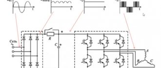
IPM modules allow direct connection to microcontrollers, converting microcontroller output signals into high-power, high-voltage signals in the form necessary for controlling electric motors. A single module can replace more than 30 discrete components, significantly increasing reliability and reducing product size and cost. Figure 3 shows the benefits of replacing discrete components with an intelligent module.
Rice. 3. Benefits of replacing discrete components with an intelligent module
Each intelligent module includes the following units and components:
- Three-phase IGBT bridge inverter including:
- Six IGBTs with low loss and short circuit protection circuits,
- Six freewheeling diodes with low voltage drop and smooth recovery;
- Smart shutdown function
- Comparator for protection against current exceeding the maximum permissible value during a short circuit,
- Operational amplifier to increase the sensitivity of the current sensor,
- Three integrated clamping diodes,
- Mutual shutdown function
- Blocking in case of overvoltage;
ST's IPM modules use DBC (direct-bond copper) housings and vacuum welding processes, which guarantee better heat dissipation and lower electrical resistance, allowing for higher power densities and increased system reliability.
Scope of use
Today, IGBT transistors are used in networks with voltage ratings up to 6.5 kW, while ensuring safe and reliable operation of electrical equipment. It is possible to use an inverter, variable frequency drives, welding machines and pulse current regulators.
Heavy-duty IGBT varieties are used in powerful control drives for trolleybuses and electric locomotives. Their use makes it possible to increase efficiency, ensuring the smoothest possible operation of equipment, promptly controlling the output of electric motors to their full power. Power transistors are used in high voltage circuits. They are used in circuits for household air conditioners, dishwashers, power supplies in telecommunications equipment, and in automobile ignitions.
Packaging and designation system for Gen6 transistors
6th generation transistors are available in standardized packages for SMD mounting (D2PAK) and through-hole mounting - TO-220, TO-247 (with standard and extended leads), as well as Super TO-247 with improved heat dissipation. Extended pins can be useful for specific placement of power components in the design (impossibility of installing a heatsink directly on the board, the need for specific pin molding, etc.).
The Super TO‑247 (aka TO‑274) package has lower thermal resistance and better conducts heat away from the die and from the package itself. The case occupies the same area as a standard TO-247, while simultaneously providing the optimal thermal characteristics and load capacity of the larger TO-264 case. Super TO‑247 does not have a mounting hole, and for tight contact of the housing with the radiator, a mounting clip is used, which presses the transistor and ensures reliable thermal contact of the surface of the transistor housing with the surface of the radiator [3]. Transistors with an operating current of up to 240 A (IRGPS4067DPBF) are available in Super TO-247 packages.
In Fig. Figure 4 shows the notation system used to designate 6th generation IGBT transistors from IR.
Rice. 4. 6th generation transistor designation system
Functionality check
Inspection and testing of IGBT semiconductors is carried out in the presence of faults in electrical devices. This test is carried out using a multitester, ringing the collectors and electrodes with the emitter in two directions. This will allow you to establish the functionality of the transistor and eliminate the lack of a short circuit. When checking, it is necessary to negatively charge the gate input using COM type multimeter probes.
To check the correct operation of the transistor at the input and output of the gate, charge the capacitance with the positive pole. This charging is performed by briefly touching the gate with a probe, after which the potential difference between the collector and emitter is checked. These potentials should not have a discrepancy of more than 1.5 Volts. If a powerful IGBT is being tested, and the tester is not enough for a positive charge, a supply voltage of up to 15 Volts is applied to the gate.
Gate breakdown
The gate is the most sensitive element of the IGBT module, so appropriate precautions must be taken. Gate breakdown is associated with the destruction of a thin gate dielectric and occurs at a gate voltage of 70–80 V. The maximum permissible gate-emitter voltage during operation is limited to ± 20 V. Nevertheless, gate breakdown remains a fairly common type of damage, which occurs even among experienced consumers .
Very often, soldering irons operating from a 220 V network are used to install IGBT modules. In this case, there is always the possibility of breakdown of the insulation in the soldering iron and an unacceptably high voltage reaching the module gate, which will lead to breakdown of the gate.
Another reason for gate damage is unreliable contacts to the control terminals. If in the finished device, in the presence of a high collector-emitter voltage, a contact failure or a break in the emitter control pin occurs, then voltage oscillations in the control circuit and high-frequency oscillations of the collector current may occur, which in turn, through the capacitance between the collector and the gate, cause an increase in voltage in gate circuits are above the maximum permissible value.
To avoid such troubles, the following requirements must be met:
- presence of antistatic coating at workplaces;
- mandatory presence of antistatic bracelets connected to grounding for personnel;
- the presence of galvanically isolated and grounded soldering irons;
- ensuring reliable connection of control pins to modules.
Powerful modules
Power transistors are manufactured not only as individual semiconductors, but also as assembled, ready-to-use modules. Such devices are part of powerful frequency converters for controlling electric motors. In each specific case, the diagram and principle of operation of the module will vary depending on its type and purpose. Most often, such devices use a bridge made of two power transistors.
Stable IGBT operation is ensured at a frequency of 150 kilohertz. As the operating frequency increases, losses may increase, which negatively affects the stability of electrical appliances. Power transistors exhibit all their advantages and capabilities when used with a voltage of more than 400 Volts. Therefore, such semiconductors are most often used in industrial equipment and high-voltage electrical appliances.
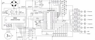
IGBT module for frequency converter
IGBT modules are connected to the control circuit using drivers, since the modules do not have built-in drivers. These are special integrated circuits that allow you to effectively drive IGBT gates and extract maximum efficiency from them. The main thing for which drivers are needed is to reduce the switching times of IGBTs to the limit, and thereby bring them closer to the ideal switch from electrical engineering textbooks. Then, coordinate them electrically with the control circuit, including providing galvanic isolation if necessary.
If external IGBT modules are used to amplify the frequency converter, then all that remains is to connect the driver outputs to them. The module diagram for the frequency converter is shown below:
The module is screwed onto a cooling aluminum radiator through heat-conducting lead paste or special ceramic gaskets. These surfaces must lie strictly in the same plane and be completely clean during assembly! Otherwise, sufficient heat dissipation will not be ensured. By the way, about temperature. The module has a built-in thermistor temperature sensor (terminals 22 and 23). The operating temperature in the module should not exceed 100°C. To remove sufficient current, additional loops are made on the power contacts (the module is made for soldering).
Contacts 1,2,3; 4,5,6; 7,8,9 are connected to a three-phase supply network.
Contacts 38,39,40 are the positive bus of the network rectifier, and contacts 41,42,43 are negative.
Contacts 33,34,35 are the positive bus of the output inverter bridge, and contacts 30,31,32 are negative. The last four listed groups, as well as pin 29, group 36,37 form the outputs for the DC link.
Contacts 10, 28 are used to connect to the driver that controls the operation of the output phase of the frequency converter. A similar role is played by groups 14, 26 and 18, 24 for the two remaining phases. Contacts 11, 12, 13 are the output of one phase of the inverter, and groups 15,16,17 and 19,20,21 are the outputs of the other two phases.
Correct PWM timing diagrams and sufficient efficiency of the drivers, which must cope with the charging and discharging of the transistor's gate capacitance, are the key to the fact that the motor will rotate at all and nothing will burn out. Therefore, the inverter bridge must first be powered from a low-power DC source with current limitation and make sure, using an oscilloscope, that there are no through currents, that the “sine” generated by the bridge is correct, that the phase shift is correct, at all frequencies that the converter produces. The control power in the frequency converter is also supplied in a laboratory manner.
The module temperature feedback signal must also be correct. When heating the module in any way within 20...80°C, it is necessary to control its actual temperature with an accurate thermometer. Then find the item with the corresponding parameter in the converter menu and check it.
If we make sure that the drivers reliably control the module, and the temperature feedback signal does not contain errors, then we can do the installation, assemble the DC link and then check again on a low-power motor, through fuses designed for the appropriate current, included in every phase.