Imported amplifiers very often use a powerful complementary pair 2SA and 2SC. We will consider them later in a detailed study of the circuit of an amplifier stage with a common emitter.
Capacitor Cp is a separating capacitor. If it is chosen correctly, the output voltage will be significantly higher than the input.
The current-voltage characteristic of the zener diode is shown in Fig. Bipolar transistors
Based on the operating frequency, transistors are divided into low-frequency - operating frequency not exceeding 3 MHz, mid-frequency - 3...30 MHz, high-frequency - over 30 MHz.
Figure 3.
The author of the article proposed regulating the rotation frequency of the commutator motor by changing the duration of the pulses in the control winding of the op-amp.
But the parameters of germanium transistors were unstable; their biggest drawback should be considered low operating temperature - no more
Although the transition layers are based on the same principle, the transistor is an asymmetrical device.
TRANSISTOR CONNECTION DIAGRAMS. EMITTER REPEATER [Radio Amateur TV 42]
Characteristics of a transistor connected according to the circuit
Only diffusion movement of electrons occurs through the base, since there is no action of the electric field there. The transistor has only three terminals, so to implement a four-terminal network, one of the terminals must be connected to both the input and output of the amplifier. A positive type of charge, or hole, is formed at the site of the released electron. The power supply voltage and load must remain the same for both measurements.
Conclusion Semiconductor elements are used in electrical signal conversion circuits. Although the transition layers are based on the same principle, the transistor is an asymmetrical device.
The active mode of the transistor is the normal mode of operation of the transistor. In this case, the transistor parameters do not play any role here at all. Firstly, the gain of the cascade depends on the specific instance of the transistor: if you replaced the transistor during repair, select the bias again, bring it to the operating point.
If the base current drops, then the collector current will also decrease - the person will correct it using a rheostat.
The operation of the amplifier is clearly visible in the timing diagrams. Figure 2. How does a transistor work? TTL logic / Gain mode. Animated educational 2D video. / Lesson 1
See also: Energy audit of an enterprise: why and when it is carried out
Step-by-step instructions for checking with a multimeter
Before starting the test, first of all, the structure of the triode device is determined, which is indicated by the emitter junction arrow. When the direction of the arrow points towards the base, then this is the PNP variant, the direction opposite to the base indicates NPN conductivity.
Testing a PNP transistor with a multimeter consists of the following sequential operations:
- We check the reverse resistance; to do this, we connect the “positive” probe of the device to its base.
- The emitter junction is tested; for this we connect the “negative” probe to the emitter.
- To check the collector, move the negative probe onto it.
The results of these measurements should show a resistance within the value of “1”.
To check direct resistance, swap the probes:
- We attach the “negative” probe of the device to the base.
- We alternately move the “positive” probe from the emitter to the collector.
- On the multimeter screen, the resistance readings should be from 500 to 1200 Ohms.
These readings indicate that the transitions are not broken, the transistor is technically sound.
Many amateurs have difficulty identifying the base, and, accordingly, the collector or emitter. Some advise starting to determine the base, regardless of the type of structure, in this way: alternately connecting the black probe of the multimeter to the first electrode, and the red probe alternately to the second and third.
The base will be detected when the voltage across the device begins to drop. This means that one of the transistor pairs has been found - “base-emitter” or “base-collector”. Next, you need to determine the location of the second pair in the same way. The common electrode of these pairs will be the base.
It will be interesting➡ Twilight switches
Verification methods
Any repair of electronics and electrical equipment begins with an external inspection, and then proceeds to measurements. This approach allows you to localize most faults. To find a varistor on the board, look at the figure below - this is what varistors look like. Sometimes they can be confused with capacitors, but can be distinguished by their markings.
If the element is burnt out and the markings cannot be read, look at this information on the device diagram. On the board and in the diagram it can be designated by the letters RU. The conventional graphic symbol looks like this.
There are three ways to test a varistor quickly and easily:
- Visual inspection.
- Call. This can be done with a multimeter or any other device that has a continuity test function.
- Resistance measurement. This can be done with a high-range ohmmeter, multimeter or megger.
A varistor fails when a large or prolonged current passes through it. Then the energy is dissipated in the form of heat, and if its amount is greater than that determined by the design, the element burns out. The housing of these components is made of a hard dielectric material, such as ceramic or epoxy coating. Therefore, when it fails, the integrity of the outer coating is most often damaged.
You can visually check the varistor for functionality - there should be no cracks on it, as in the photo:
The next method is to check the varistor with a tester in continuity mode. This cannot be done in the circuit, because the dialing can work through parallel-connected elements. Therefore, you need to unsolder at least one of its legs from the board.
Important: you should not check the elements for serviceability without desoldering them from the board - this may give false readings from the measuring instruments. Since in the normal state (without voltage applied to the terminals) the resistance of the varistor is high, it should not ring through. The test is performed in both directions, that is, by swapping the multimeter probes twice
The test is performed in both directions, that is, by swapping the multimeter probes twice
Since in the normal state (without voltage applied to the terminals) the resistance of the varistor is high, it should not ring through. The test is performed in both directions, that is, by swapping the multimeter probes twice.
On most multimeters, the continuity mode is combined with the diode testing mode. It can be found by the diode icon on the mode selector scale. If there is a sound indication sign next to it, it probably also has a dial tone.
Another way to test a varistor for breakdown with a multimeter is to measure the resistance. You need to set the device to the maximum measurement limit, in most devices this is 2 MOhms (megaohms, designated as 2M or 2000K). The resistance must be equal to infinity. In practice, it can be lower, within 1-2 MOhm.
Interesting! The same can be done with a megaohmmeter, but not everyone has one. It is worth noting that the voltage at the megohmmeter terminals should not exceed the classification voltage of the component being tested.
This ends the available methods for checking a varistor. This time, the multimeter will help the radio amateur find the faulty element, as in a large number of other cases. Although in practice a multimeter is not always needed in this matter, because the matter rarely goes beyond a visual inspection. Replace the burnt element with a new one, designed for voltage and with a diameter no less than the burnt one, otherwise it will burn out even faster than the previous one.
Scheme with a common base
In this case, the input resistance is very small, and the output resistance is high.
Let us recall that the reactance of a capacitor Xc, Ohm, can be calculated using the formula: For direct current, the reactance of capacitors tends to infinity. The signal requires a load in the output circuit. In addition to bipolar ones, there are unipolar field-effect transistors, which use only one type of carrier - electrons or holes. The active mode of a transistor is the normal mode of operation of the transistor. The uppermost characteristic at point A intersects with the direct load, after which, with a further increase in IB, the collector current no longer changes.
This amplification is carried out using the energy of the power source. A voltage of 0.6V is the voltage at the B-E junction, and you should not forget about it when calculating!
Circuits for switching on bipolar transistors when combining cutoff and saturation modes make it possible to create electronic switches with their help. Advantages of a cascade based on a circuit with a common emitter: 1. In order to better understand how emitter stabilization works, it is necessary to consider the circuit for switching on a transistor with a common collector OK.
Connection diagram for a bipolar transistor with a common collector
Operation of a transistor in switch mode Before studying the operation of a transistor in signal amplification mode, it is worth remembering that transistors are often used in switch mode. Emitter-follower common-collector circuits are used to match the high output impedance of the signal source with the low input impedance of the load. The performance of the BT depends on the thickness of the base layer of the BT. Now let's trace the operation of this circuit itself: power supply 1.
Hence the large spread in the gain of transistors taken even from the same box, or the same batch. And the model range is constantly increasing, allowing us to solve almost all the tasks set by the developers. Figure 7. Therefore, for DC amplifiers, the lower cutoff frequency of the gain is zero, no coupling capacitors are required, and special measures must be taken to separate the stages. The figure shows a diagram of the operation of a transistor in switching mode.
The emitter follower uses a transistor circuit with a common collector OK. Power is the product of current and voltage, but since the voltage does not change, the power increases only due to the current! The base is the control electrode. Bipolar transistors. Operating principle.
Why do you need a transistor?
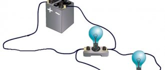
I often have a question: why do we need a transistor? Why not connect the LED and resistor directly to the battery?
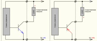
The advantage of a transistor is that you can use a small current or voltage to control a much larger current and voltage.
This is very useful if you want to control things like motors, high power LEDs, speakers, relays and more using a microcontroller/Raspberry Pi/Arduino. The output of the microcontroller can only provide a few milliamps at 5V. So if you want to control, for example, a 230V street light, you cannot do it directly with the microcontroller
You can use a relay instead. But even a relay usually requires more current than the microcontroller output can provide. Therefore you will need a transistor to drive the relay:
It will be interesting➡ The strength of electric current and everything about it
Characteristics of a transistor connected according to the OE circuit:
The main elements of the circuit are: a transistor, a resistor RL and an amplifier output circuit with external power.
Due to the insignificant thickness of the micron layer and the large concentration gradient of negatively charged particles, almost all of them fall into the collector area, although the base resistance is quite high. Where can I buy transistors? Transistors are rightfully considered one of the great discoveries of mankind.
When operating in active mode, the voltage at the emitter junction is direct, and at the collector junction it is reverse. It is also designated as Outcomes from the above, the transistor can operate in four modes: Transistor cutoff mode - in this mode, the base-emitter junction is closed, this can happen when the base-emitter voltage is insufficient. Firstly, the gain of the cascade depends on the specific instance of the transistor: if you replaced the transistor during repair, select the bias again, bring it to the operating point.
The answer may or may not be yes. Since the collector current is tens of times greater than the base current, this explains the fact that the current gain is tens of units. Circuit with a common collector OK. Practical options for connecting transistors of the p-p-p and p-p-p structure are shown in Fig. For some reason, this name almost never appears in the literature, but among radio engineers and radio amateurs it is used everywhere, everyone immediately understands what we are talking about.
NPN transistor operation:
Now that the n side of the diode has the most electrons and the p side has the most holes, all voltage connections are arranged as forward and reverse bias respectively. The emitter base junction is configured as reverse bias and the collector base junction is configured as forward bias. The depletion region of this emitter-base region is narrower compared to the depletion region at the collector-base intersection.
Since the junction is reverse biased (emitter), the holes flow from the power supply to the N junction. The electron then moves towards p. Here some electron is neutralized. The remaining electrons move towards n. The voltage drop relative to the emitter and base is VBE as the input side.
In N-type emitters, the charge carriers are mainly electrons. Consequently, electrons are transferred through the N-type emitters to the P-type base. The current will flow through the emitter-base or EB junction. This current is known as emitter current (Ie). Here, the emitter current (IE) flows from the output side and flows in two directions; one is IB and the other is IC. So we can write:
It will be interesting➡ Schemes and methods of connecting electric motors
IE=IB+IC
However, the base region is relatively thin and lightly doped. Consequently, most of the electrons pass through the base region and only a few of them recombine with the available holes. The base current is minimal compared to the emitter current. Typically this is up to 5% of the total emitter current.
The current flowing from the rest of the electrons is called collector current (IC). YC is relatively high compared to baseline (IB).
Applications of PNP transistors:
- PNP transistors are used as switches i.e. analog switches, emergency buttons, etc. They are used when emergency shutdown is required.
- These types of transistors are used in current source circuits, i.e., by taking advantage of the characteristics of the current flowing from the collector.
- Used in amplification circuits.
- They are used in paired Darlington circuits.
- PNP transistors are used in heavy-duty motors for current control and in various robot and microcontroller development applications.
Next
Miscellaneous AC Voltage. Does the outlet have direct current or alternating current?