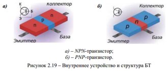
Bipolar transistor - an electronic semiconductor device, one of the types of transistors, designed to amplify, generate and convert electrical signals. The transistor is called bipolar because two types of charge carriers - electrons and holes - are simultaneously involved in the operation of the device. This differs from a unipolar (field-effect) transistor, in which only one type of charge carrier is involved.
The principle of operation of both types of transistors is similar to the operation of a water tap that regulates the flow of water, only a flow of electrons passes through the transistor. In bipolar transistors, two currents pass through the device - the main “large” current, and the control “small” current. The main current power depends on the control power. With field-effect transistors, only one current passes through the device, the power of which depends on the electromagnetic field. In this article we will take a closer look at the operation of a bipolar transistor.
Bipolar transistor design.
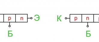
A bipolar transistor consists of three semiconductor layers and two PN junctions. PNP and NPN transistors are distinguished by the type of alternation of hole and electronic conductivity. It's like two diodes connected face to face or vice versa.
A bipolar transistor has three contacts (electrodes). The contact coming out of the central layer is called the base. The outermost electrodes are called collector and emitter. The base layer is very thin relative to the collector and emitter. In addition to this, the semiconductor regions at the edges of the transistor are asymmetrical. The semiconductor layer on the collector side is slightly thicker than on the emitter side. This is necessary for the transistor to operate correctly.
Operation of a bipolar transistor.
Let's consider the physical processes occurring during operation of a bipolar transistor. Let's take the NPN model as an example. The principle of operation of a PNP transistor is similar, only the polarity of the voltage between the collector and emitter will be opposite.
As already mentioned in the article about the types of conductivity in semiconductors, a P-type substance contains positively charged ions - holes. N-type substance is saturated with negatively charged electrons. In a transistor, the concentration of electrons in the N region significantly exceeds the concentration of holes in the P region.
Let's connect a voltage source between the collector and emitter VCE (VCE). Under its action, electrons from the upper N part will begin to be attracted to the plus and collect near the collector. However, current will not be able to flow because the electric field of the voltage source does not reach the emitter. This is prevented by a thick layer of collector semiconductor plus a layer of base semiconductor.
Now let's connect the voltage between the base and emitter VBE, but significantly lower than VCE (for silicon transistors the minimum required VBE is 0.6V). Since the layer P is very thin, plus a voltage source connected to the base, it will be able to “reach” with its electric field the N region of the emitter. Under its influence, electrons will be directed to the base. Some of them will begin to fill the holes located there (recombine). The other part will not find a free hole, because the concentration of holes in the base is much lower than the concentration of electrons in the emitter.
As a result, the central layer of the base is enriched with free electrons. Most of them will go towards the collector, since the voltage is much higher there. This is also facilitated by the very small thickness of the central layer. Some part of the electrons, although much smaller, will still flow towards the plus side of the base.
As a result, we get two currents: a small one - from the base to the emitter of the IBE, and a large one - from the collector to the emitter of the ICE.
If you increase the voltage at the base, then even more electrons will accumulate in the P layer. As a result, the base current will increase slightly and the collector current will increase significantly. Thus, with a small change in the base current IB, the collector current IC changes greatly. This is how the signal is amplified in a bipolar transistor . The ratio of the collector current IC to the base current IB is called the current gain. It is designated β, hfe or h21e, depending on the specifics of the calculations carried out with the transistor.
β = IC/IB
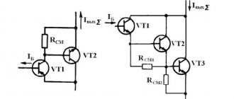
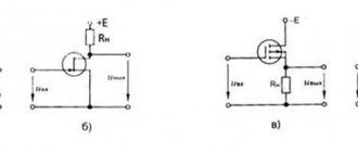
With common collector (OK)
A common collector circuit is often called an “emitter follower”. It has a high input (about >200 kOhm) and low output (about <10 kOhm) resistance. This circuit does not provide voltage gain. A common collector circuit is used in the input stages of amplifiers to match two amplifier stages, of which the previous one has a high output, and the subsequent one, usually the output stage, has a low input impedance. The OK circuit does not change the phase of the input signal. The output voltage at the output of the circuit with OK (Figure 3, common collector) practically repeats the voltage at the base of the transistor, taking into account the magnitude of the slight voltage drop at the emitter-base junction, hence the name “emitter follower”. Due to the high current gain, the OK circuit is also used to control the currents of various devices, such as solenoids.
The simplest bipolar transistor amplifier
Let us consider in more detail the principle of signal amplification in the electrical plane using the example of a circuit. Let me make a reservation in advance that this scheme is not entirely correct. No one connects a DC voltage source directly to an AC source. But in this case, it will be easier and more clear to understand the amplification mechanism itself using a bipolar transistor. Also, the calculation technique itself in the example below is somewhat simplified.
1.Description of the main elements of the circuit
So, let’s say we have a transistor with a gain of 200 (β = 200). On the collector side, we will connect a relatively powerful 20V power source, due to the energy of which amplification will occur. From the base of the transistor we connect a weak 2V power source. We will connect to it in series an alternating voltage source in the form of a sine wave, with an oscillation amplitude of 0.1V. This will be a signal that needs to be amplified. The resistor Rb near the base is necessary in order to limit the current coming from the signal source, which usually has low power.
Calculation of base input current Ib
Now let's calculate the base current Ib. Since we are dealing with alternating voltage, we need to calculate two current values - at the maximum voltage (Vmax) and minimum (Vmin). Let's call these current values Ibmax and Ibmin, respectively.
Also, in order to calculate the base current, you need to know the base-emitter voltage VBE. There is one PN junction between the base and emitter. It turns out that the base current “meets” the semiconductor diode on its path. The voltage at which a semiconductor diode begins to conduct is about 0.6V. We will not go into details of the current-voltage characteristics of the diode, and for simplicity of calculations we will take an approximate model, according to which the voltage on the current-carrying diode is always 0.6V. This means that the voltage between base and emitter VBE = 0.6V. And since the emitter is connected to ground (VE = 0), the voltage from base to ground is also 0.6V (VB = 0.6V).
Let's calculate Ibmax and Ibmin using Ohm's law:
Calculation of collector output current IC
Now, knowing the gain (β = 200), you can easily calculate the maximum and minimum values of the collector current (Icmax and Icmin).
Calculation of output voltage Vout
It remains to calculate the voltage at the output of our amplifier Vout. In this circuit, this is the voltage at the collector VC.
The collector current flows through the resistor Rc, which we have already calculated. It remains to substitute the values:
Analysis of results
As can be seen from the results, VCmax turned out to be less than VCmin. This is because the voltage across resistor VRc is subtracted from the supply voltage VCC. However, in most cases this does not matter, since we are interested in the variable component of the signal - the amplitude, which has increased from 0.1V to 1V. The frequency and sinusoidal shape of the signal have not changed. Of course, a Vout/Vin ratio of ten times is far from the best indicator for an amplifier, but it is quite suitable for illustrating the amplification process.
So, let's summarize the principle of operation of an amplifier based on a bipolar transistor. A current Ib flows through the base, carrying DC and AC components. A constant component is needed so that the PN junction between the base and emitter begins to conduct - “opens”. The variable component is, in fact, the signal itself (useful information). The collector-emitter current inside the transistor is the result of the base current multiplied by the gain β. In turn, the voltage across the resistor Rc above the collector is the result of multiplying the amplified collector current by the resistor value.
Thus, the Vout pin receives a signal with an increased oscillation amplitude, but with the same shape and frequency. It is important to emphasize that the transistor takes energy for amplification from the VCC power source. If the supply voltage is insufficient, the transistor will not be able to operate fully, and the output signal may be distorted.
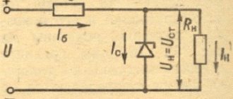
Fixed Base Current Bias Circuit
The simplest bias circuit uses a base bias resistor between the base and the base battery Vbias. Using an existing Vpit source instead of a new bias source is very convenient. An example of this bias circuit is shown in the audio amplifier stage of a detector receiver in the RF Circuits section of Chapter 9. Note the resistor between the base and battery terminal. A similar diagram is shown in the figure below.
Write the equation of Kirchhoff's voltage law for a circuit that includes a battery, RB and the voltage drop VBE across the transistor junction in the figure below. Please note that we use the notation Voffset, although in fact it is Vpit. If the coefficient β is large, we can make the approximation that IK = IE. For silicon transistors VBE ≅ 0.7 V.
Fixed Base Current Bias Circuit
\[V_{offset} - I_B R_B - V_{BE} = 0\]
\[V_{offset} - V_{BE} = I_B R_B\]
\[I_B = { V_{offset} - V_{BE} \over R_B }\]
\[I_E = (\beta + 1)I_B \approx \beta I_B\]
\[I_E = { V_{displacement} - V_{BE} \over R_B / \beta }\]
The β coefficient of small-signal transistors is typically in the range of 100–300. Assuming we have a β=100 transistor, what value of base bias resistor would be required to achieve 1mA emitter current?
Solving the IE equation to determine RB and substituting the values of β, Voffset, VBE and IE will give the result 930 kOhm. The closest standard value is 910 kOhm.
\(\beta = 100 \qquad V_{offset} = 10 V \qquad I_K \approx I_E = 1 mA \)
\[R_B = { V_{offset} - V_{BE} \over I_E / \beta } = { 10 - 0.7 \over 1 mA / 100 } = 930 kOhm \]
What will be the emitter current with a 910 kOhm resistor? What happens to the emitter current if we replace the transistor with a random one with β=300?
\(\beta = 100 \qquad V_{offset} = 10 V \qquad R_B = 910 kOhm \qquad V_{BE} = 0.7 V\)
\[I_E = { V_{offset} - V_{BE} \over R_B / \beta } = { 10 - 0.7 \over 910 kOhm / 100 } = 1.02 mA \]
\(\beta = 300\)
\[I_E = { 10 - 0.7 \over 910 kOhm / 300 } = 3.07 mA \]
When using a standard 910 kOhm resistor, the emitter current will change slightly. However, when β changes from 100 to 300, the emitter current triples. This is unacceptable for a power amplifier if we expect the collector voltage to vary from near Vsupply to near ground. However, for low level signals from microvolts to about a volt, the bias point can be centered at β equal to the square root of (100 300), which is equal to 173. The bias point will still drift over a significant range. However, low level signals will not be clipped.
A fixed base current bias circuit is inherently unsuitable for the large emitter currents used in power amplifiers. The emitter current in a bias circuit with a fixed base current is not temperature stable. Temperature runaway is the result of high emitter current, which causes an increase in temperature, which causes an increase in emitter current, which will further increase the temperature.
Operating modes of a bipolar transistor
In accordance with the voltage levels on the electrodes of the transistor, there are four modes of its operation:
- Cut off mode.
- Active mode.
- Saturation mode.
- Inverse mode (reverse mode).
Cut-off mode
When the base-emitter voltage is lower than 0.6V - 0.7V, the PN junction between the base and emitter is closed. In this state, the transistor has no base current. As a result, there will be no collector current either, since there are no free electrons in the base ready to move towards the collector voltage. It turns out that the transistor is, as it were, locked, and they say that it is in cutoff mode.
Active mode
In active mode, the voltage at the base is sufficient for the PN junction between the base and emitter to open. In this state, the transistor has base and collector currents. The collector current equals the base current multiplied by the gain. That is, the active mode is the normal operating mode of the transistor, which is used for amplification.
Saturation mode
Sometimes the base current may be too high. As a result, the supply power is simply not enough to provide such a magnitude of collector current that would correspond to the gain of the transistor. In saturation mode, the collector current will be the maximum that the power supply can provide and will not depend on the base current. In this state, the transistor is not able to amplify the signal, since the collector current does not respond to changes in the base current.
In saturation mode, the conductivity of the transistor is maximum, and it is more suitable for the function of a switch (switch) in the “on” state. Similarly, in the cut-off mode, the conductivity of the transistor is minimal, and this corresponds to the switch in the off state.
Inverse mode
In this mode, the collector and emitter change roles: the collector PN junction is biased in the forward direction, and the emitter junction is biased in the opposite direction. As a result, current flows from the base to the collector. The collector semiconductor region is asymmetrical to the emitter, and the gain in inverse mode is lower than in normal active mode. The transistor is designed in such a way that it operates as efficiently as possible in active mode. Therefore, the transistor is practically not used in inverse mode.
Add a link to a discussion of the article on the forum
RadioKot >Training >Analog technology >Basics of electronics >
| Article tags: | Add a tag |
Scary word - Transistor
Author: Published 11/13/2006
Well, actually, having passed seven boring and useless chapters about all sorts of crap =), we finally got to the most interesting and exciting. Before the transistor.
Modern electronics could not exist if not for this element! After all, even the most sophisticated microcircuit, somewhere in the depths of its silicone soul, consists of the same transistors. Only very small ones.
A transistor is an amplifying element. It amplifies the weak energy of the signal supplied to it due to the energy of an additional power source.
Let me explain. We have all traveled at least once by train, commuter train, or at least tram. When the train slows down, you can always hear a characteristic hissing sound. This operates the pneumatic brake actuator. In other words, compressed air goes from the tank to the brakes. The brake pads are connected to the piston. When compressed air begins to press on the piston, the piston moves forward and presses the pads tightly against the wheel. The train slows down... Why does air begin to flow onto the piston? This is probably what the driver wants. He opens the valve in his cabin and air flows. Everything is indecently simple!
A small explanatory picture:
Now let's ask ourselves, would the driver be able to stop the train if the brake lever was directly connected to the brake pads? Probably, not. No matter how strong he is, a person cannot stop a train. And compressed air does this easily, you just need to open the valve.
Let's see what happened: the driver spends little energy pressing the brake lever. The valve opens and a powerful stream of compressed air, with much more energy, presses the brake pads. That is, the valve can be called a reinforcing element that enhances the weak energy expended by a person due to the strong energy of compressed air.
I dare to assure you that everything is absolutely the same in a transistor. Only it is not compressed air that passes through it, but electric current. The transistor has three terminals: collector, emitter and base.
A strong current flows between the collector and the emitter, it is called the collector current (Ik), between the base and the emitter there is a weak control current of the base (Ib). The magnitude of the collector current depends on the magnitude of the base current, just as the pressure of compressed air depends on how open the valve is. Moreover, the collector current is always greater than the base current by a certain number of times. This value is called the current gain, denoted h21e
. For different types of transistors, this value ranges from units to hundreds of times.
So, the current gain is the ratio of the collector current to the base current:
h21e = Ik / Ib
In order to calculate the collector current, you need to multiply the base current by the gain:
Ik = Ib * h21e
Let's draw a diagram.
In this circuit, a transistor controls the brightness of the light bulb. In other words, it regulates the current flowing through the light bulb. Since the light bulb is connected to the collector of the transistor, the current flowing through it is the collector current.
The base control current is limited by resistor R1. Knowing this current and the gain of the transistor (h21e), you can easily find out the collector current. On the other hand, knowing what collector current we need, we can always calculate the base current and select the appropriate resistor.
Let's do some math
.
Problem:
Let our light bulb consume a current of 0.33 A, and the transistor has h21e = 100. What base current is needed for the light bulb to burn at full intensity? And what will be the resistance R1?
Full heat is when the current consumption is equal to the rated current. Rated - 0.33 A. Thus, the required collector current is 0.33 A. The base current must be less than the collector current by a factor of h21e. That is, 100 times. That is, it should be equal to 0.33/100 = 0.0033A = 3.3 mA. Hurray, we decided!!!
Now it remains to calculate the resistance of the resistor in the base circuit. We calculate (according to Ohm's law):
R = U/I
U - we know - this is the supply voltage, 9V I - just found - 0.0033 A
Arithmetic, 2nd grade: R = 9/0.0033 = 2700 Ohm = 2.7 kOhm.
Answer: resistor value = 2.7 kOhm
Just? Still would! But don’t flatter yourself. Further - worse! =)
In the next few paragraphs we'll talk about things other than the transistor. But after this, we will definitely return to it, with new interesting knowledge. And we will be able to use this element more widely.
<<—Let’s remember what we’ve covered—Let’s move on—>>
| What do you think of this article? | Did this device work for you? | |
| 150 | 7 | 1 |
| 13 | 4 |