Additional functions of voltage stabilizers
In addition to the main function of voltage stabilizers - stabilization, there is also the following minimum set of functions and parameters:
Maybe this will be interesting too?
- Output voltage analysis. The stabilizer must be equipped with an information (digital or pointer) display that shows the output voltage. If the stabilizer has an input voltage analysis function, this will be additional useful information.
- At higher ratings (usually from 3000 VA), the “Bypass” function is installed - a function in an electronic device (signal processing, voltage stabilization, etc.) that allows you to switch the input signal directly to the output, bypassing all functional blocks. That is, the ability to turn on the network bypassing the voltage stabilizer. If the voltage has returned to normal or you do not need a stabilizer now, press the lever up and the voltage goes bypassing the stabilization blocks.
- Types of fastening of voltage stabilizers There are two types of fastening of voltage stabilizers - floor and wall versions. Floor-standing design means that the stabilizer is located on the floor or shelf. This arrangement is not always convenient, because especially large denominations cannot be placed on a shelf due to their weight, and they occupy quite large areas on the floor. When mounted, the stabilizers are made flatter for the convenience of customers. In principle, they can also be used in a floor-standing version, only often the information part of the display is in this case “upside down” towards the user.
- Many models on the voltage stabilizer market use a delay button. This is done so that if the voltage in the network disappears or temporarily goes beyond the operating range, the equipment will come to a rest position during this delay time before the next turn on. In many stabilizers, the delay button is offered in several ranges -6, 90, 120 sec. In more modern models, the delay has already become automatic and when it is turned on, it shows the consumer on the display the time the stabilizer is turned on in the form of a countdown.
Surge protection
In the case of medium and high power power supplies intended for industrial applications, surge immunity according to the EU standard IEC / EN61000-4-5 ± 2 / ± 4 kV is an important parameter. Proper circuit design in this area requires the use of a three-stage protection scheme.
The input terminals of the power supply are protected by semiconductor elements (powerful zener diodes), which provide fast operation, but at the same time are not able to absorb large amounts of energy from voltage surges. The central part is usually a varistor, which has a medium operating speed and is capable of absorbing medium energy surges.
The elements of the gas discharger are located closest to the terminals of the 220 V network, capable of absorbing large discharge power, but slowly, since ionization of the gas takes a long time. The individual blocks are connected by chokes that limit the rate of voltage rise in individual sections.
Not every power supply has such extensive input protection circuits, but they are critical in terms of quality, especially in applications operating over a wide range of input voltages, such as 85 - 264 VAC and 120 - 370 VDC. The same applies to output protection (overcurrent, short circuit, thermal stress, undervoltage). Manufacturers do not always implement a complete set of such schemes.
Three-stage overvoltage protection
Overvoltages, unstable mains voltage, a large number of harmonics can lead to the instantaneous supply voltage at the power supply terminals, being a superposition of all phenomena, exceeding the permissible value and the structure will be damaged.
Therefore, for important devices, you should choose power supplies with the widest possible range of permissible input voltage. An example is the Mornsun LS and LD converters - they operate in the range of 90 - 528 V AC and 100 - 745 V DC.
DIY adjustable power supply
A power supply is a necessary thing for every radio amateur, because to power electronic homemade products you need a regulated power source with a stabilized output voltage from 1.2 to 30 volts and a current of up to 10A, as well as built-in short circuit protection. The circuit shown in this figure is built from the minimum number of available and inexpensive parts.
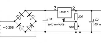
Scheme of an regulated power supply on an LM317 stabilizer with short-circuit protection
The LM317 IC is an adjustable voltage regulator with built-in short circuit protection. The LM317 voltage stabilizer is designed for a current of no more than 1.5A, so a powerful MJE13009 transistor is added to the circuit, capable of passing through itself a really high current of up to 10A, according to the datasheet, a maximum of 12A. When you rotate the knob of the variable resistor P1 by 5K, the voltage at the output of the power supply changes.
There are also two shunt resistors R1 and R2 with a resistance of 200 Ohms, through which the microcircuit determines the output voltage and compares it with the input voltage. 10K resistor R3 discharges capacitor C1 after the power supply is turned off. The circuit is powered by voltage from 12 to 35 volts. The current strength will depend on the power of the transformer or switching power supply.
I drew this diagram at the request of novice radio amateurs who assemble circuits using wall-mounted installations.
Scheme of an regulated power supply with short-circuit protection on LM317
It is advisable to carry out the assembly on a printed circuit board, so it will be beautiful and neat.
Printed circuit board of the regulated power supply on the LM317 voltage regulator
The printed circuit board is made for imported transistors, so if you need to install a Soviet one, the transistor will have to be unfolded and connected with wires. The MJE13009 transistor can be replaced with the MJE13007 from the Soviet KT805, KT808, KT819 and other npn structure transistors, it all depends on the current you need. It is advisable to reinforce the power paths of the printed circuit board with solder or thin copper wire. The LM317 voltage stabilizer and the transistor must be installed on a radiator with sufficient area for cooling; a good option is, of course, a radiator from a computer processor.
It is advisable to screw a diode bridge there. Don't forget to insulate the LM317 from the heatsink with a plastic washer and a heat conductive gasket, otherwise there will be a big boom. Almost any diode bridge can be installed with a current of at least 10A. Personally, I installed the GBJ2510 at 25A with double the power reserve, it will be twice as cool and reliable.
And now the most interesting part... Testing the power supply for strength.
I connected the voltage regulator to a power source with a voltage of 32 volts and an output current of 10A. Without load, the voltage drop at the output of the regulator is only 3V. Then I connected two series-connected halogen lamps H4 55 W 12V, the lamp filaments were connected together to create a maximum load, the result was 220 W. The voltage dropped by 7V, the nominal voltage of the power supply was 32V. The current consumed by four halogen lamp filaments was 9A.
The radiator began to heat up quickly, after 5 minutes the temperature rose to 65C°. Therefore, when removing heavy loads, I recommend installing a fan. You can connect it according to this diagram. You can not install the diode bridge and capacitor, but connect the L7812CV voltage stabilizer directly to capacitor C1 of the regulated power supply.
Connection diagram of the fan to the power supply
What happens to the power supply if there is a short circuit?
In the event of a short circuit, the voltage at the output of the regulator is reduced to 1 volt, and the current is equal to the current of the power source, in my case 10A. In this state, with good cooling, the unit can remain for a long time; after the short circuit is eliminated, the voltage is automatically restored to the limit set by the variable resistor P1. During the 10-minute short-circuit test, no parts of the power supply were damaged.
Radio components for assembling an adjustable power supply on LM317
- Voltage stabilizer LM317
- Diode bridge GBJ2501, 2502, 2504, 2506, 2508, 2510 and other similar ones designed for a current of at least 10A
- Capacitor C1 4700mf 50V
- Resistors R1, R2 200 Ohm, R3 10K all resistors with a power of 0.25 W
- Variable resistor P1 5K
- Transistor MJE13007, MJE13009, KT805, KT808, KT819 and other npn structures
Friends, I wish you good luck and good mood! See you in new articles!
I recommend watching a video on how to make an adjustable power supply with your own hands
About some types of power supplies
Sometimes it happens that a power supply can produce several voltages; they are often called multi-channel. For example, this is a computer power supply, which is necessary to protect equipment from power surges.
Laboratory power supplies are designed for use during experiments on a special breadboard. The block must have sufficient capabilities, because it is often used for setting up a variety of structures.
Recently, power supplies have been produced that are designed for one fixed voltage. Such a block reliably protects equipment from increased output voltage. This protection is not complicated in its structure; only a few details are needed to implement it. Most often it can be found in some amateur radio designs.
Electromechanical (servo-drive) devices
If it is elevated, it moves down. The role of the current collector slider in stabilizers is performed by graphite brushes. They maintain the output voltage with high accuracy (up to 2%), and its adjustment is smooth. These are their main advantages. Some stabilizers, for example, those produced, use not one, but two graphite brushes. This increases the contact area. This device regulates voltage faster.
Some electromechanical models with a power of over 30 kW can be equipped with an additional transformer. Despite the presence of moving parts, devices of this type operate silently. They have a high overload capacity.
By choosing this equipment, you can significantly simplify the calculation: add a quarter of it to the obtained average power of the equipment and thus obtain the characteristics of the future stabilizer. This means that it is permissible to take the minimum reserve of stabilizer power and pay a lower purchase price.
| Manufacturer | power, kWt | Input voltage, W |
| Resanta | 0,5-100 | 140-260240-430 (three-phase) |
| Elitech | 0,5-30 | 160-250280-430 |
| Caliber | 0,5-30 | 160-250 |
| Sturm | 0,5-30 | 140-250 |
The mains voltage is adjusted using a slider that moves along the winding. At the same time, different numbers of turns are used. We all studied at school, and some of us may have dealt with a rheostat in physics lessons.
An electromechanical voltage stabilizer works on this similar principle. Only the slider is moved not manually, but using an electric motor called a servo drive. It is simply necessary to know the structure of these devices if you want to make a 220V voltage stabilizer with your own hands according to the diagram.
Electromechanical devices are highly reliable and provide smooth voltage regulation. Characteristic advantages:
- Stabilizers work under any load.
- The resource is significantly greater than that of other analogues.
- Affordable cost (half lower than electronic devices)
Unfortunately, with all the advantages there are also disadvantages:
- Due to the mechanical design, the response delay is very noticeable.
- Such devices use carbon contacts, which are subject to natural wear and tear over time.
- The presence of noise during operation, although it is practically inaudible.
- Small operating range 140-260 V.
The current is adjusted by connecting more turns of the transformer. In case the device does not have time to react in a timely manner to excessive voltage, a relay is provided in the stabilizer device.
A stabilizer made independently has its pros and cons, which you should definitely know about. Main advantages:
- low cost;
- maintainability;
- independent diagnostics.
The most obvious advantage is its low cost. All parts will need to be purchased separately, and this is still incomparable with ready-made stabilizers.
If any element of the purchased voltage stabilizer fails, it is unlikely that you can replace it yourself. In this case, all that remains is to call a technician to your home or take him to a service center. Even if you have some knowledge in the field of electrical engineering, finding the right part is not so easy. It’s a completely different matter if the device was made by hand. All the details are already familiar and to buy a new one, just visit the store.
If anyone has previously assembled a 220V 10kW voltage stabilizer circuit with their own hands, it means that the person already understands many of the intricacies. This means that identifying the malfunction will not be difficult.
Design, ergonomics and intuitive perception of the design: personal opinion
After opening the package, two power modules and an instruction manual were found inside.
On the front side of the blocks there is a “Network” LED, which warns by its glow that the module is entering operating mode, and the designation of the terminals for connection is shown:
- AC input circuits (primary circuit): phase L, working zero N and grounding;
- output circuits of stabilized supply voltage of the secondary circuit: plus and minus 12/24 volt network, ground.
There are no digital markings for terminals accepted at the factory. It is also not entirely clear to which terminals the “+” and “–” input circuits need to be connected when the device is powered from DC voltage operational circuits.
This information is provided in the Manual on page #4.
“Plus” should be connected to the working zero terminal, and minus – to the phase.
However, if you carry out installation according to the terminal markings, you may make a mistake:
- The numbering is given when looking at the board from below, and not from above, as we usually look at such a source when connecting it;
- numbers 4, 5 and 6 are missing.
I admit that for some reason it is more convenient for the manufacturer to carry out the technological process this way. But the end user should be more careful.
Mounting the power supply on a DIN rail
The modular unit is created according to the most modern DIN rail mounting standards. All this is clearly visible in the photo of the underside of the product.
This method allows for quick installation not only inside ordinary electrical panels (apartment, house), but also on relay protection panels with DIN rails installed in relay rooms.
It is worth noting that the design of the power supply is far from universal and can lead to problems when used on old Soviet-style relay protection and automation panels, which continue to be used en masse.
Two of their types (solid body and rack mounting of relay protection devices), shown in the photo below, will require the installation of an additional DIN rail.
If the manufacturer had made a couple of holes in the case, or soldered fastening nuts into its plastic, then the process of installing the blocks on solid horizontal or vertical planes would have been significantly simplified.
This can hardly be considered a serious design flaw, because such a power source can be placed on a shelf even without preliminary fastening.
Principle of operation
How does our network voltage stabilizer, which is easy to make with your own hands, work?
After the power is turned on, capacitor C1 is in a discharged state, transistor VT2 is open, and VT2 is closed. Transistor VT3 is also closed. It is through it that current will be supplied to each LED and triac optotron.
Since this transistor is off, the LEDs are not lit, each triac is off, and the load is off. At this time, electric current passes through resistor R1 and enters C1. Next, this capacitor is charged.
The delay interval lasts only three seconds. During this time, all transient processes are carried out, and after completion, the Schmitt trigger is triggered, the basis of which is transistors VT1 and VT2.
Next, the third transistor opens and the load is turned on.
The voltage that comes out from the third winding T1 is rectified by the diode VD2 and capacitor C2. Next, the current passes through the divider R13…14. From R14, a voltage whose level is proportional to the number of volts in the network is included in each non-inverting input of the comparators.
The number of comparators is eight and they are all located on chips DA2 and DA3. At the same moment, a constant reference current enters the inverting input of each comparator. It is supplied by resistor dividers R15…23.
After this, the controller comes into play, which processes the signal at the input of each comparator.
- https://electricadom.com/stabilizator-napryazheniya-kak-vse-sdelat-svoimi-rukami-video.html
- https://amperof.ru/sovety-elektrika/sxema-stabilizatora-napryazheniya-220v.html
- https://lifehacker.ru/how-to-make-steadycam/
- https://ostabilizatore.ru/shema-stabilizatora-naprjazhenija-220v-svoimi-rukami.html
- https://fb.ru/article/360616/shema-stabilizatora-napryajeniya-v-svoimi-rukami-dlya-doma
- https://generatorvolt.ru/ehlektrogenerator/kak-sobrat-stabilizator-napryazheniya-svoimi-rukami.html
Minimizing inrush current
The input circuit of most low-power switching power supplies includes a bridge rectifier and a filter capacitor, which together provide the filtered DC voltage needed to power the electronics in the power supply. When such a power supply is connected to the network, a temporary overload occurs due to the fact that if the sinusoidal wave of the mains voltage does not pass through zero at the moment the voltage is turned on, this capacitor on the rectifier has a small resistance and its charging causes a short pulse of high-intensity current, even several tens peak ampere.
NTC thermistor limiting maximum inrush current
This current is usually limited by an NTC thermistor in series with the power line, which initially has a resistance high enough to reduce inrush current, heats up during operation and its resistance decreases, reducing power loss. Typically the resulting overcurrent reduction is up to 10 times less.
But not all low-power power supplies and converters have this component in the case, because manufacturers, in an effort to get a low price, get rid of it, considering it an unnecessary element. Therefore, when choosing a power supply, it is worth checking whether NTC is installed in the case. The figure shows a typical location of the thermistor in the electrical circuit of a power supply such as the LHxx-10B.
Stabilization of household voltage
The desire to provide stabilized voltage to the household network is an obvious phenomenon. This approach ensures the safety of the equipment in use, often expensive and constantly needed on the farm. And in general, the stabilization factor is the key to increased safety in the operation of electrical networks.
For domestic purposes, a stabilizer is most often purchased for a gas boiler, the automation of which requires connection to a power supply, for a refrigerator, pumping equipment, split systems and similar consumers.
Industrial design of a mains voltage stabilizer, which is easy to purchase on the market. The range of such equipment is huge, but there is always the opportunity to make your own design
This problem can be solved in different ways, the simplest of which is to buy a powerful voltage stabilizer manufactured industrially.
There are a lot of offers of voltage stabilizers on the commercial market. However, purchasing options are often limited by the cost of devices or other factors. Accordingly, an alternative to purchasing is to assemble a voltage stabilizer yourself from available electronic components.
Provided you have the appropriate skills and knowledge of electrical installation, the theory of electrical engineering (electronics), wiring circuits and soldering elements, a homemade voltage stabilizer can be implemented and successfully used in practice. There are such examples.
Stabilization equipment made with your own hands from available and inexpensive radio components may look something like this. The chassis and housing can be selected from old industrial equipment (for example, from an oscilloscope)
Total Power Output
Few power supply buyers are aware that the specified maximum output power is not always available over the full operating temperature range and for every input voltage. Many simple power supplies also have problems with stability of operation without load or at low power (Pmax less than 10%).
The power supply must have redundancy and allow temporary overload, which is important when turning on inductive loads or others that consume more power when turned on.
Even when the circuit is working correctly, you need to make sure that at low input voltage and high temperature it will still work stable, because many power supplies available on the market have problems with this point.
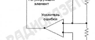
Functional diagrams by type of control circuit
The switching voltage stabilizer is an automatic regulation system. The setting parameter for the control loop is the reference voltage, which is compared with the output voltage of the stabilizer. Depending on the mismatch signal, the control device changes the ratio of the durations of the open and closed states of the key.
In the block diagrams presented below, three functional units can be distinguished: a switch (1), an energy storage device (2) (sometimes called a filter) and a control circuit. In this case, the switch (1) and the energy storage device (2) together form the power part of the voltage stabilizer, which, together with the control circuit, form a control loop. There are three schemes based on the type of control circuit.
With Schmitt trigger
A voltage stabilizer with a Schmitt trigger is also called a relay or on-off regulator. In it, the output voltage is compared with the lower and upper thresholds of the Schmitt trigger (4 and 3) using a comparator (4), which is usually the input part of the Schmitt trigger. When the switch (1) is closed, the input voltage is supplied to the energy storage device (2), the output voltage increases, and after reaching the upper threshold Umax
The Schmitt trigger switches to a state that opens the switch (1).
The accumulated energy is consumed in the load, while the voltage at the output of the stabilizer drops, and after reaching the lower operating threshold Umin
, the Schmitt trigger switches to a state that closes the switch. The described process is then repeated periodically. As a result, a pulsating voltage is formed at the output, the ripple range of which depends on the difference in the Schmitt trigger thresholds.
Such a stabilizer is characterized by a relatively large, fundamentally irremovable voltage ripple at the load and a variable conversion frequency, depending on both the input voltage and the load current.
With pulse width modulation
Block diagram of a voltage stabilizer with PWM
As in the previous circuit, during operation the energy storage device (2) is either connected to the input voltage or transfers the accumulated energy to the load
As a result, the output has a certain average voltage value, which depends on the input voltage and the duty cycle of the key control pulses (1). The operational amplifier subtractor (4) compares the output voltage with the reference voltage (6) and amplifies the difference, which is fed to the modulator (3). If the output voltage is less than the reference voltage, then the modulator increases the ratio of the time the switch is open to the period of the clock generator (5)
When the input voltage or load current changes, the duty cycle of the switch control pulses changes in such a way as to ensure a minimum difference between the output and reference voltage
If the output voltage is less than the reference voltage, then the modulator increases the ratio of the time the switch is open to the period of the clock generator (5)
When the input voltage or load current changes, the duty cycle of the switch control pulses changes in such a way as to ensure a minimum difference between the output and reference voltage
In such a stabilizer, the conversion frequency does not depend on the input voltage and load current and is determined by the frequency of the clock generator.
With pulse frequency modulation
With this control method, the pulse that opens the key has a constant duration, and the pulse repetition rate depends on the mismatch signal between the reference and output voltages. As the load current increases or the input voltage decreases, the frequency increases. The switch can be controlled, for example, using a monostable multivibrator (one-shot) with a controlled trigger frequency.
THE ARTICLE WAS PREPARED BASED ON THE BOOK BY A. V. GOLOVKOV and V. B LYUBITSKY “POWER SUPPLY FOR SYSTEM MODULES OF THE IBM PC-XT/AT TYPE” BY THE PUBLISHING HOUSE “LAD&N”
STABILIZATION OF OUTPUT VOLTAGES OF PULSE POWER UNITS
The output voltage stabilization circuit in the class of UPS under consideration is a closed automatic control loop (Fig. 31). This loop includes: • control circuit 8; • matching preamplifier stage 9; • control transformer DT; • power stage 2; • power pulse transformer RT; • rectifier unit 3; • interchannel communication choke 4; • filter block 5; • feedback voltage divider 6; • reference voltage divider 7. The control circuit 8 contains the following functional units: • mismatch signal amplifier 8.1 with correction circuit Zk; • PWM comparator (modulator) 8.2; • sawtooth voltage generator (oscillator) 8.3; • source of stabilized reference voltage Uref 8.4. During operation, the mismatch signal amplifier 8.1 compares the output signal of voltage divider b with the reference voltage of divider 7. The amplified mismatch signal is supplied to the pulse-width modulator 8.2, which controls the pre-final stage of the power amplifier 9, which, in turn, supplies a modulated control signal to the power stage converter 2 via control transformer DT. The power cascade is powered using a transformerless circuit. The alternating voltage of the supply network is rectified by the network rectifier 1 and supplied to the power stage, where it is smoothed out by capacitors of the capacitive rack. Part of the output voltage of the stabilizer is compared with a constant reference voltage and then the resulting difference (mismatch signal) is amplified with the introduction of appropriate compensation. The 8.2 pulse-width modulator converts the analog control signal into a width-modulated signal with a variable duty cycle. In the class of UPS under consideration, the modulator circuit compares the signal coming from the output of the error signal amplifier with the sawtooth voltage, which is obtained from a special generator 8.3.
Figure 31. Regulatory loop of a typical switching power supply based on the TL494 control chip.
The main transfer functions of the UPS are the input-output function, which characterizes the ability of the circuit to suppress input noise and ripple and not let them pass to the output, and the control-output function, which characterizes the degree of change in output voltages at different duty cycles. In a closed-loop system, the duty cycle of the pulses is determined by the amplified and compensated error signal. Let's explain this in more detail. Let's say that some disturbing influence (for example, an increase in current consumption in the load) initially caused a deviation of the output voltage by a certain amount towards a decrease. Therefore, the amount of mismatch between the reference voltage and the feedback signal changes. Due to this, the width of the output pulses of the modulating circuit 8-2 increases. Therefore, the output voltage increases, but does not reach its previous value, but is set at a level slightly lower than before the disturbance, and remains at this new level until the increased current consumption in the load stops. The newly established level of the output voltage provides the magnitude of the error signal, which, being amplified by the error amplifier 8.1, determines the new width of the control pulse that supports this new level of output voltage. In other words, the system enters a new state of dynamic equilibrium, but with a larger mismatch signal than before and a different (larger) width of control pulses. It is quite obvious that the greater the gain of the error amplifier, the smaller the change in the output voltage, which will determine the width of the control pulses necessary to maintain this voltage. Therefore, it would seem that it would be desirable to have the gain factor of an 8.1 amplifier as high as possible. However, the magnitude of the gain is limited by the condition of stable operation of the entire control loop as a whole. The value of the feedback loop gain is equal to the product of the gain factors of the standard units included in the feedback loop, and its phase shift is equal to the sum of the phase shifts of the standard units. Therefore, the gain in the feedback loop and its phase determine the stability of the system and the possibility of generation occurring in it. In order for the system to operate stably, the frequency response and phase response of the amplifier 8.1 is circuit-corrected using the correction circuit Zk, which is switched on as a negative feedback link covering the error amplifier 8.1. In this case, the configuration of the Zk chain ensures the necessary dependence of the depth of this OOS on the frequency of the amplified signal. Simply put, Zk is a circuit through which negative frequency-dependent feedback is introduced. Let us explain in more detail the physical meaning of the inclusion of this very important chain. As is known from theory, for generation to occur in a closed system, two conditions must be met. The first of these conditions is called phase balance and is that the total phase shift introduced by all parts of the closed system at a given frequency should be equal to 360 degrees. Then the feedback turns into positive and the possibility of self-excitation of the system appears. The second condition, called amplitude balance, is that the loop gain at a given frequency be greater than 1. When both of these conditions are met simultaneously, generation occurs in a closed control loop. In relation to the UPS output voltage control loop, it will look approximately the same. The phase shift introduced by each element of the control loop is not constant, but depends on frequency. Therefore, there is necessarily a certain frequency at which the total phase shift of the control loop becomes equal to 360 degrees. It is at this frequency that generation can occur. This possibility is realized if the loop gain, which, as noted, is determined by the product of the gains of all parts of the loop, has a value greater than 1 at the specified frequency. From what has been said it is clear that in order to avoid the occurrence of such parasitic generation, there is only one way. Since the loop gain is determined mainly by the error amplifier 8.1, this way is to adjust the frequency response of the error amplifier (and therefore the frequency response of the entire control loop as a whole) so that at the frequency where the total phase shift in the loop becomes equal to 360 degrees , the loop gain would be less than 1. The function of such a change in the frequency response of the amplifier 8.1 is performed by the Zk correction circuit, which is usually performed in the form of an integrating RC link. Despite the fact that the Zk compensation circuit is a very small part of the complete UPS circuit, it is the “key” for stable operation of the system. Let us explain all of the above in relation to the class of UPS under consideration based on the TL494 control chip. Stabilization of output voltages is carried out using the pulse width modulation method. Its essence lies in the fact that the feedback signal, proportional to the voltage level in the +5V channel, when galvanically applied to the non-inverting input of the error amplifier DA3 (pin 1 of the TL494 microcircuit), determines the width of the output pulse of the microcircuit and changes it in accordance with deviations in the output voltage channel +5Here is the nominal value. Let us consider the dynamics of the stabilization process. Suppose that under the influence of some destabilizing factor (for example, an abrupt change in load), the output voltage in the +5V channel has decreased. Then the level of the feedback signal at the non-inverting input of the error amplifier DA3 will decrease. Consequently, the amplifier's output voltage will decrease. Therefore, the width of the output pulses of the microcircuit at pins 8 and 11 will increase. This means the open state time will increase during the period of the inverter’s power key transistors. Consequently, for a larger part of the period than before, an increasing current will flow through the primary winding of the power pulse transformer. Consequently, for a larger part of the period than before, an increasing magnetic flux will exist in the core of the transformer, which means that for longer than before, the EMF induced by this flow will act on the secondary windings of this transformer. In other words, the EMF pulses on the secondary side of the power transformer will become wider ( with a constant tracking period). Therefore, the constant component isolated by the smoothing filter from the pulse sequence after rectification increases, i.e. the output voltage of the +5V channel will increase, returning to the nominal value. When the output voltage increases +5V, the processes in the circuit will be reversed. Stabilization of the output voltages of the remaining channels can be carried out differently in different circuits. The traditional circuit solution is to use the group stabilization method. To do this, a special interchannel communication element is included in the block circuit, which is usually a multi-winding inductor. In this case, a change in any output voltage leads, thanks to the electromagnetic connection between the windings of the group stabilization inductor, to a corresponding change in the output voltage +5V with the subsequent activation of the PWM mechanism. The group stabilization choke usually consists of four windings (one winding in each output channel of the power supply unit), wound on one ring ferrite core and connected in phase. In this case, the inductor performs two functions in the circuit: • the function of smoothing the ripple of the rectified voltage - in this case, each winding for its channel represents a smoothing filter inductor and works like a regular inductor; • the function of inter-channel communication with group stabilization - in this case, thanks to electromagnetic communication through a common core, the inductor works as a transformer, transmitting changes in the magnitude of currents flowing through the windings of the +12V, -12V and -5V channels to the winding of the +5V channel. Let's explain this in more detail. A feature of the operation of a UPS in a personal computer is that the current consumed from the UPS depends on the operation currently being performed, i.e. changes abruptly. Let, for example, at a given moment in time the current load in the +12V channel increase abruptly. An increase in current through the inductor winding connected in the +12V channel causes an increase in the magnetic flux in the inductor core. A change in the magnetic flux, in turn, induces an EMF in all other windings of the inductor, the polarity of which (due to the in-phase winding of the inductor windings) in all channels turns out to be turned on counter to the output voltages of the rectifiers. Therefore, the output voltages of all channels (including the +5 V channel) decrease. The feedback signal from the +5 V channel is galvanically transmitted to the PWM circuit, which increases the duration of the output control pulses. Therefore, the output voltages of all UPS channels increase, returning to the nominal value. When the current load changes in other channels, the circuit operates similarly. However, the stabilization coefficient of output voltages in all channels except the +5V channel is low, i.e. stabilization of voltages +12V, -12V and -5V will be worse than in the +5V channel, which is directly “monitored”. This method of complete group stabilization is used, for example, in the KYP-150W UPS (Fig. 27). There are options for switching power supplies with incomplete group stabilization, such as LPS-02-150ХТ. In the circuit of this UPS, only three output voltages (+5V, +12V and -12V) are “connected” through a group stabilization choke. The -5V voltage is stabilized in a different way - using a linear integrated stabilizer type 7905 (Fig. 28). The communication choke in this case is made of three windings. The mechanism for using a group stabilization choke is used in the vast majority of cases, but occasionally there are UPSs in which this mechanism is not used. In such UPSs, at the output of the -5V and -12V generation channel there are voltage stabilizers of the type 7905 and 7912 (much less often - 7805 and 7812), and feedback to the IC1 microcircuit at pin 1 is provided through a resistive divider-sensor from the output voltages +5V and +12V (Fig. 32). The feedback signal in this case is total, because its level is determined by the voltage levels on both buses, and therefore both output voltages (+5V and +12V) are stabilized by the PWM method. And finally, there are UPS variants in which the -5V voltage is obtained from -12V using an integral stabilizer, and the -12V voltage itself is not stabilized at all. In the last two types of circuits, there is no multi-winding inductor for interchannel communication. Stabilization circuits may also differ in the way the feedback signal and reference voltage are supplied to the inputs of the error amplifier DA3. At the same time, adjustments can be installed in these circuits, allowing you to change the output voltage levels of the UPS when setting it up. Since the voltage error amplifier DA3 is a differential amplifier, i.e. amplifies the difference between the signals supplied to its inputs 1 and 2, then the adjustment can be in the circuit of both one and the other input. In this case, the non-inverting input DA3 (pin 1 of the chip) is always used to supply a feedback signal, and the inverting input (pin 2 of the chip) is always used to supply the reference voltage. This is explained by the fact that for normal operation of the control loop, the output voltage of the error amplifier DA3 must change in phase with the feedback signal. The output voltages of the block can be adjusted in two ways: • by changing the level of the feedback signal while maintaining a constant reference voltage at pin 2; • by changing the level of the reference voltage at pin 2 while maintaining a constant level of the feedback signal at input 1. The first of these cases is illustrated in Fig. 32, and the second - Fig. 33.
Figure 32. Adjusting the output voltage level of the PS-200B UPS.
Figure 33. Adjusting the output voltage level of the LPS-02-150XT UPS.
Figure 34. Adjusting the output voltage level of the Appis UPS.
Figure 35. Adjusting the output voltage level of the GT-200W UPS.
However, the most common case is when there is no adjustment to influence the output voltages of the unit. In this case, the voltage at any of inputs 1 or 2 is selected arbitrarily in the range from +2.5 to +5 V, and the voltage at the remaining input is selected using a high-impedance shunt resistor so that the unit produces the output voltages specified in the passport at the nominal load mode. Rice. 35 illustrates the case of selecting the reference voltage level, Fig. 34 - shows the case of selecting the level of the feedback signal. It was previously noted that the instability of the output voltage under the influence of any destabilizing factors (changes in load current, supply voltage and ambient temperature) could be reduced by increasing the gain of the feedback circuit (gain of amplifier DA3). However, the maximum value of the gain DA3 is limited by the stability condition. Since both the UPS and the load contain reactive elements (inductance or capacitance) that accumulate energy, energy is redistributed between these elements in transient modes. This circumstance may lead to the fact that, with certain parameters of the elements, the transient process of establishing the output voltages of the UPS will take on the character of undamped oscillations, or the amount of overregulation in the transient mode will reach unacceptable values.
Figure 36. Transient processes (oscillatory and aperiodic) of the UPS output voltage with an abrupt change in the load current (a) and input voltage (b).
In Fig. Figure 36 shows the transient processes of the output voltage with an abrupt change in the load current and input voltage. The UPS operates stably if the output voltage returns to its steady value after the disturbance that brought it out of its original state ceases (Fig. 37a).
Figure 37. UPS output voltage transients in stable (a) and unstable (b) systems.
If this condition is not met, then the system is unstable (Fig. 37.6). Ensuring the stability of a switching power supply is a necessary condition for its normal functioning. The transient process, depending on the UPS parameters, is oscillatory or aperiodic in nature, while the UPS output voltage has a certain overshoot value and transient process time. The deviation of the output voltage from the nominal value is detected in the measuring element of the feedback circuit (in the UPS under consideration, a resistive divider connected to the +5V output voltage bus is used as a measuring element). Due to the inertia of the control loop, the nominal value of the output voltage is set with a certain delay. In this case, the control circuit by inertia will continue to act in the same direction for some time. As a result, overshoot occurs, i.e. deviation of the output voltage from its nominal value in the direction opposite to the original deviation. The control circuit again changes the output voltage in the opposite direction, etc. In order to ensure the stability of the UPS output voltage regulation loop with a minimum duration of the transient process, the amplitude-frequency characteristic of the error amplifier DA3 is subject to correction. This is done using RC circuits connected as negative feedback circuits surrounding the DA3 amplifier. Examples of such corrective chains are shown in Fig. 38.
Figure 38. Examples of configuration of correcting RC chains for the voltage error amplifier DA3.
To reduce the level of noise generation, aperiodic RC circuits are installed on the secondary side of the switching power supply. Let's take a closer look at the principle of their operation. The transient process of the current through the rectifier diodes at the moments of switching occurs in the form of shock excitation (Fig. 39, a).
Figure 39. Voltage timing diagrams on the reverse resistance recovery diode: a) - without an RC circuit; b) - in the presence of an RC chain.
This process creates electromagnetic interference with a frequency of tens of megahertz. Through the interwinding capacitances of the transformer and the interturn capacitances of the smoothing filter choke, these noises penetrate into the primary network and to the output of the UPS. To reduce this interference, it is necessary to change the nature of the transient process in the region of the reverse current of the rectifier diodes so that it is aperiodic in nature. The advantage of an aperiodic transient process over an oscillatory one is that the amplitude of the initial surge is reduced due to the charge of the capacitor of the RC circuit, as well as its faster attenuation due to the resistor of this circuit, which reduces the quality factor of the parasitic oscillatory circuit. An effective method for ensuring the aperiodic nature of the transient process is to connect an RC circuit in parallel with the transformer windings and rectifier diodes, as shown in Fig. 30. When using an RC circuit, the transient process of changing the current through the diode in the mode of restoring its reverse resistance has the form shown in Fig. 39.6.
CONTENTS OF A CYCLE OF ARTICLES ON SWITCH POWER SUPPLY SUPPLY:
| BASIC PARAMETERS OF SWITCH POWER SUPPLY FOR IBM | The main parameters of switching power supplies are considered, the connector pinout is given, the principle of operation on mains voltage is 110 and 220 volts, |
| MANAGING POWER SWITCHES OF A SWITCHING POWER SUPPLY USING TL494 | The TL494 microcircuit, switching circuit and use cases for controlling power switches of switching power supplies are described in detail. |
| MANAGING POWER SWITCHES OF A SWITCHING POWER SUPPLY USING TL494 | The main methods for controlling the basic circuits of power transistors in switching power supplies and options for constructing secondary power rectifiers are described. |
| STABILIZATION OF OUTPUT VOLTAGES OF PULSE POWER UNITS | Options for using error amplifiers TL494 to stabilize output voltages are described, and the operating principle of a group stabilization choke is described. |
| PROTECTION SCHEMES | Several options for constructing systems for protecting pulsed power supplies from overload are described. |
| "SLOW START" SCHEME | The principles of forming a soft start and generating POWER GOOD voltage are described |
| EXAMPLE OF CONSTRUCTION OF ONE OF THE PULSE POWER SUPPLY SUPPLY | A complete description of the circuit diagram and its operation of a switching power supply |
Site administration address
Manufacturing stages
To assemble a 220V voltage stabilizer for your home with your own hands, you first need to prepare a printed circuit board measuring 115x90 mm. It is made of foil fiberglass. The layout of the parts can be printed on a laser printer and transferred to the board using an iron.
Let's watch the video, a homemade simple device:
electrical circuit diagram
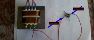
Next we move on to assembling the transformers. For one such element you will need:
- magnetic core with a cross-sectional area of 1.87 cm²;
- three PEV-2 cables.
The first wire is used to create one winding, and its diameter is 0.064 mm. The number of turns should be 8669.
The two remaining wires will be needed to make other windings. They differ from the first one in diameter being 0.185 mm. The number of turns for these windings will be 522.
If you want to simplify your task, you can use two ready-made TPK-2-2 12V transformers. They are connected in series.
In the case of making these parts yourself, after one of them is ready, they move on to creating the second. It will require a toroidal magnetic circuit. For the winding, choose the same PEV-2 as in the first case, only the number of turns will be 455.
Also in the second transformer you will have to make 7 taps. Moreover, for the first three, a wire with a diameter of 3 mm is used, and for the rest, buses with a cross-section of 18 mm² are used. This will help prevent the transformer from heating up during operation.
connection of two transformers
It is better to purchase all other components for a device you create yourself in a store. Once everything you need has been purchased, you can begin assembly. It is best to start by installing a microcircuit that acts as a controller on a heat sink, which is made of aluminum platinum with an area of more than 15 cm². Triacs are also mounted on it. Moreover, the heat sink on which they are supposed to be installed must have a cooling surface.
Next you need to install LEDs on the board. Moreover, it is better to choose blinking ones. If it is not possible to arrange them according to the diagram, then you can place them on the side where the printed conductors are located.
If assembling a 220V triac voltage stabilizer with your own hands seems complicated to you, then you can opt for a simpler linear model. It will have similar properties.
The effectiveness of a handmade product
What pushes a person to make this or that device? Most often - its high cost. And in this sense, a voltage stabilizer assembled with your own hands is, of course, superior to a factory model.
In addition, all the parts for such a device were previously purchased in the store, so if they fail, you can always find a similar one.
If we compare the reliability of a stabilizer assembled with our own hands and manufactured at an enterprise, then the advantage is on the side of factory models. At home, it is almost impossible to develop a model with high performance, since there is no special measuring equipment.
Conclusion
There are different types of voltage stabilizers, and some of them are quite possible to make with your own hands. But to do this, you will have to understand the nuances of the operation of the equipment, purchase the necessary components and carry out their proper installation. If you are not confident in your abilities, then the best option is to purchase a factory-made device. Such a stabilizer costs more, but the quality is significantly superior to models assembled independently.
Do-it-yourself electronic load up to 500 W
Simple Electronic Load for Beginners
Author: KomSoft Published 02/11/2015 Created using KotoEd.
I’ll start with a quote: “Usually during the manufacture (as well as during repair) of power supplies or voltage converters, it is necessary to check their performance under load. And then the search begins. Everything that is at hand is used: various incandescent light bulbs, old vacuum tubes, powerful resistors and the like. Selecting the required load in this way is an incredibly costly task (both in terms of time and nerves). (Couldn't have said it better! I've encountered this problem myself.) Instead, it's very convenient to use an electronically adjustable load. No, no, you don't need to buy anything. Even a schoolboy can do such a load. All you need is a powerful field switch, an op-amp, a few resistors and a larger heatsink. The scheme is more than simple and, nevertheless, works great.” — https://radiohlam.ru/raznoe/nagruzka.htm
This article is a preface to a more complex device and is intended for those who constantly shuffle powerful resistors and light bulbs used as a load, but do not yet have the knowledge (experience, determination) to assemble complex circuits.
It all started with the above article and this diagram with calculations (for a description I refer you to the original source):
Based on this circuit, a device was assembled that was almost identical to the author’s, which faithfully served for a couple of years at a voltage of up to 20-25V. It can be seen that the low-resistance resistor Rti is assembled from as many as four! assistants.
Unfortunately, when testing the next block and supplying a voltage of more than 30V from it, the load burned out - the field switch broke through, most likely due to the gate-drain voltage being exceeded. In addition, the current in this circuit is very dependent on the applied voltage. Therefore, the circuit was slightly modified - stabilizers for the op-amp supply voltage, reference voltage, and an indicator of high dangerous (for the circuit) voltage were added.
There's not much to describe here. A reference voltage source is assembled on the VD2 zener diode, which operates quite tolerably (sufficient for such tasks) at voltages from 7 to 30V. When the voltage is less than 5V, the zener diode VD2 does not enter mode and, due to a decrease in the voltage on it, as well as insufficient voltage at the output U1, the maximum current set by the load is reduced.
Operational amplifier U1, transistor Q1 and resistors R6, R7 form a source of stable current, the value of which is regulated by changing the voltage supplied from resistor R3.
Auxiliary elements of the scheme are:
- diode VD1 protects the circuit from improper power supply;
- integrated stabilizer U2, which limits the supply voltage of the microcircuit, the fan and the voltage at the gate of the field-effect transistor;
- LED HL1 indicating power supply;
- HL2 LED indicating dangerously high input voltage.
Of course, with an input voltage of less than 13V, the voltage at the output of the integrated stabilizer will also be reduced, but this does not significantly affect the operation of the circuit.
Board and location of parts (view from the parts side, one blue jumper):
The board drawing is in the attached file, no need to mirror it.
The device was assembled from what was at hand, mixed with power supplies, monitors and even old Soviet radio components. A field-effect transistor of almost any such structure with a current of more than 5A and a voltage of more than 30V, for example IRFZ34, 44 and similar ones - whatever is at hand. The diode assembly is from the AT(X) power supply. The radiator and fan are from the processor (larger). To supply voltage, it has connectors - a standard Molex from a hard drive (male) and two screw ones.
The minimum current is determined by the fan current. The load quite reliably holds 12V/4A, i.e. power dissipation is about 50W. within 10 minutes. After this, the smell makes it clear that there is not enough cooling. At high voltages, it is advisable not to set high currents, so as not to exceed this power and prevent the transistor from overheating, or use a larger radiator and fan.
Thus, the result was a simple device assembled from “junk”, which does not require a separate power source, does not contain pulse converters, and in 95% of cases meets the needs of the radio amateur when checking and adjusting power supplies.
And I’ll tell you about a similar load with a modular structure and expanded functionality next time.
What you need to connect
In addition to the stabilizer itself, you will need a number of additional materials:
three-core cable VVGnG-Ls
The cross-section of the wire must be exactly the same as on your input cable, which comes to the main input switch or circuit breaker. Since the entire load of the house will go through it.
three position switch
This switch, unlike simple ones, has three states:
123
You can also use a regular modular circuit breaker, but with this scheme, if you need to disconnect from the stabilizer, you will have to completely de-energize the entire house each time and reconnect the wires.
There is, of course, a bypass or transit mode, but in order to switch to it, you need to follow a strict sequence. This will be discussed in more detail below.
With this switch, you completely cut off the unit with one movement, and the house remains with light directly.
PUGV wire of different colors
You must clearly understand that the voltage stabilizer is installed strictly before the electric meter, and not after it.
Not a single energy supplying organization will allow you to connect in another way, no matter how much you prove that by doing so, in addition to the electrical equipment in the house, you want to protect the meter itself.
The stabilizer has its own idle speed and also consumes energy, even when operating without load (up to 30 W/h and above). And this energy must be taken into account and calculated.
The second important point is that it is highly desirable that in the circuit up to the connection point of the stabilization device there is either an RCD or a differential circuit breaker.
This is recommended by all manufacturers of popular brands Resanta, Sven, Leader, Shtil, etc.
It could be an introductory automatic differential for the whole house, it doesn’t matter. The main thing is that the equipment itself is protected from current leakage
And breakdown of the transformer windings to the housing is not such a rare thing.
Do-it-yourself powerful electronic load
The maximum input voltage is up to 60V, more is possible, it all depends on the voltage of the transistors.
Also, the electronic load is protected against polarity reversal. The maximum power dissipation is about 1500-1600W. Such a device is capable of loading almost any power source, even welding inverters, but it is important not to exceed the maximum power, and here, as mentioned above, it is 1600 W. It is worth noting that all 1600W in this case will be used for heating, so this is a fairly serious heater.
I think you'll agree that the above specifications are truly impressive for a linear load. Current loads with similar parameters are quite expensive, naturally our version will not have any special bells and whistles.
Attention!
It’s worth noting a few points right away to avoid additional questions.
Firstly,
the diagram turned out to be quite large and most likely some small details will not be visible. You will find the diagram in good quality in the project archive. Also, a link to download the archive is in the description under the author’s original video.
Secondly,
The values of some circuit elements may differ from those installed on the board, but the device will work in both cases.
Third,
the most preferred transistors TIP142 were used in the circuit, these are composite switches that are easy to operate and the driver will hardly heat up, but the total load power with the switches indicated in the diagram will be less than in this case, since the transistors used here are much more powerful .
The lower the value of this resistance, the greater the current. The specified resistor must be selected. The author conducted numerous experiments with the resulting device to find out how much power a transistor in such a package can dissipate, the maximum collector current, and how heavily the control driver will be loaded at different current values on the power transistor.
The tests were successful, and not a single transistor was damaged. Through experience, it became clear that the 32A transistors declared by the manufacturer hold up. The case is capable of dissipating 150W, and with a fan, even 200W.
The value of 200W from each transistor, you see, is quite good. And the author screwed 4 keys onto each radiator using thermal paste. In this case there are 2 such radiators.
It is worth noting that the above circuit operates in linear mode, so the transistors are open or partially closed during the process, this depends on the output voltage of the operational amplifier.
The more open the power transistor is, the greater the current in the circuit and vice versa. As mentioned above, all power is released as heat on the power transistors and current sensors, so if you want to repeat this project, first of all take care of good cooling of these circuit components. The author used fairly good aluminum radiators in the form of a bar.
The first variable is used for rough adjustment, the second, respectively, for smoother adjustment. The control board requires a low-power power supply. For example, it can be powered by batteries or accumulators. This solution will make the load completely autonomous.
The power diodes mentioned at the beginning of the article are installed at the load input. They are protected against polarity reversal. The reverse voltage and current of the diode should be selected with a double margin. In the future, the author plans to change the protection to another one, most likely using field-effect transistors.
This is how another monster was born, it’s quite difficult to come up with another name for this beast, horse radiators and power keys, brutal power, what else is needed for complete happiness. That's all for today. Thank you for attention. See you again!
Author's video:
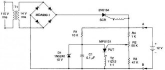
Operating principle
Let's look at how a DIY voltage stabilizer functions.
After connecting the power, capacitance C1 is in a discharge state, transistor VT1 is open, and VT2 is closed. VT3 transistor also remains closed. Through it, current flows to all LEDs and an optitron based on triacs.
Since this transistor is in a closed state, the LEDs do not light up, and each triac is closed, the load is turned off. At this moment, current flows through resistance R1 and arrives at C1. Then the capacitor begins to charge.
The shutter speed range is three seconds. During this period, all transition processes are carried out. After their completion, a Schmitt trigger based on transistors VT1 and VT2 is triggered. After this, the 3rd transistor opens and the load is connected.
The voltage coming from the 3rd winding T1 is equalized by diode VD2 and capacitance C2. Next, the current flows to the divider at resistances R13-14. From resistance R14, a voltage, the magnitude of which directly depends on the magnitude of the voltage, is included in each non-inverting comparator input.
The number of comparators becomes equal to 8. They are all made on DA2 and DA3 microcircuits. At the same time, direct current is supplied to the inverted input of the comparators, supplied using dividers R15-23. Next, the controller comes into action, receiving the input signal of each comparator.
Connection of PE line to ground
The PE protective conductor of the AC/DC power supply is connected to the metal case and structural elements of the power supply unit, since its purpose is to protect people from electric shock when touching the power supply during operation.
Good and bad way to connect the ground wire to the secondary terminals
However, it is worth noting that the PE is not connected directly to the ground of the secondary pins. Correct connection requires the use of a capacitor with a capacitance of less than 1 nF and the appropriate voltage class.
Diagram and operating principle of a diode bridge
Diode bridge diagram Fig. Highest operating rectification current.
With the advent of cheap semiconductor diodes, this circuit began to be used more and more often. The answer is shown in the following figure. They determined it without knowing anything about free electrons or holes. The result is a higher degree of smoothing with the same capacitance of the filter capacitor, increasing the efficiency of the transformer used in the rectifier. If one diode in a monolithic assembly fails, the entire assembly will have to be replaced, despite the fact that the three remaining elements may be serviceable.
The pulsations are smoothed out, and the voltage becomes close to constant. Device connection diagram On electrical diagrams and printed circuit boards, a diode rectifier is indicated by a diode icon or in Latin letters.
As the name suggests, a bridge of 4 or 6 diodes is assembled. Working with both half-waves of alternating voltage, the diode bridge compares favorably with half-wave rectifiers.
Operating principle of a diode bridge
Metals are characterized by the fact that electrons in their crystal lattice almost do not stick, fly out and dangle between the atoms of the crystal for any reason, the slightest temperature, causing the nuclei of atoms in their places to vibrate slightly, knocks out the electrons completely and en masse. If you don't have a multimeter, you can use a regular voltmeter.
In this circuit, current flows from the phase with the highest potential, through the load to the phase with the lowest potential. This ripple can be slightly reduced by using a capacitor connected in parallel to the output of the diode bridge.
Its value increases and depends only on the resistance of the p- and n-regions. Rectifier design and connection diagram To date, nothing better has been invented for full voltage rectification than a conventional diode bridge. WHAT IS A DIODE BRIDGE
What to expect from the power supply if the installer makes a mistake (input terminals are mixed up)
The idea of such a spontaneous check arose immediately after looking at the connection diagram to DC circuits.
The fact is that among the recorders of emergency processes of high-voltage equipment 110-330 kV, I came across devices powered from operational current circuits through diode isolation on the built-in terminal blocks.
It makes no difference to them what is connected at the input: “+” or “–”. Built-in diodes correct any situation, allowing you to use any connection.
At the output of Retom-21, the polarity of the output signal was changed and it was applied to the power supply under test.
It did not start and did not work.
Conclusion: it is very important to follow the specified factory connection diagram.
Transistor voltage stabilizer
Stabilizer on one zener diode
To smooth out voltage ripples and constant current at the output of the power supply, stabilizers are used. As a rule, the stabilizer is based on a zener diode. Zener diode is a semiconductor device with voltage stabilization properties. Unlike a conventional diode, it operates in reverse polarity (plus is supplied to the cathode), in avalanche breakdown mode. Due to this property of the zener diode, the voltage on it, and therefore on the load, practically does not change. The figure below shows a diagram of a simple stabilizer.
This stabilizer is suitable for powering low-power devices.
The principle of operation of the stabilizer on a zener diode
A capacitor is needed to smooth out voltage ripples; it is called a filter. A resistor is needed to smooth out current ripples and is called a damping resistor. The zener diode stabilizes the voltage across the load. For normal operation of this circuit, the supply voltage must be greater than 40...50%. The zener diode should be selected for the voltage and current we need.
Stabilizer on one transistor
To power a higher power load, a transistor is added to the circuit. An example circuit is shown below.
The principle of operation of a stabilizer on a single transistor
The chain of R1 and VT1 is already familiar to us from the previous circuit; this is the simplest stabilizer; it sets a stabilized voltage based on transistor VT2. The transistor, in turn, performs the function of a current amplifier and is a control element in this circuit. For example, as the input voltage increases, the output voltage will tend to increase. This leads to a decrease in the voltage at the emitter junction of transistor VT2, which leads to its closure. In this case, the voltage drop in the emitter-collector section increases so much that the voltage on the zener diode decreases to the original level. When the voltage drops, the stabilizer reacts in the reverse order.
Transistor stabilizer with short circuit protection
In the practice of a radio amateur, mistakes occur and a short circuit occurs. To reduce the consequences of a short circuit, consider a stabilizer circuit for two fixed voltages and with short circuit protection.
As you can see, transistor V4, diodes V6 and V7 have been added to this circuit, and a parametric stabilizer consisting of resistor R1, diodes V2, V3 is equipped with switch S2.
Operating principle of stabilizer protection
This circuit is designed for a short-circuit response current of 250...300 mA; as long as it is not exceeded, the current will pass through a voltage divider consisting of diode V7 and resistor R3. By selecting this resistor, you can adjust the protection threshold. Diode V6 will be closed and will not have any effect on the work. When the protection is triggered, diode V7 will close, and diode V6 will open and bypass the zener diode connections, while transistors V4 and V5 will close. The load current will drop to 20...30 mA. Transistor V5 should be installed on the heat sink.
Stabilizer with adjustable output voltage
When repairing or adjusting electronic devices, it is necessary to have a power supply with an adjustable output voltage. A schematic diagram of voltage-regulated stabilizers is presented below.
The principle of operation of a stabilizer with voltage regulation
A parametric stabilizer consisting of R2 and V2 stabilizes the voltage across the variable resistor R3. The voltage from this resistor is supplied to the control transistor. This transistor is connected according to the emitter follower circuit, the load of which is resistor R4. The voltage from resistor R4 is supplied to the control transistor V4, the load of which is already our powered device. Voltage regulation is carried out by variable resistor R3; if the resistor slider is in the minimum position according to the circuit, then the voltage to open transistors V3 and V4 is not enough and the output will have a minimum voltage. When the engine rotates, the transistors begin to open, which increases the voltage across the load. As the load current increases, the voltage drop across resistor R1 and lamp H1 begins to light up; at a current of 250 mA, a dim glow is observed, and at a current of 500 mA and above, a bright glow is observed. Transistor V4 should be installed on the heat sink. With an increased load of more than 500 mA, you should turn off the power supply as quickly as possible, since under prolonged maximum load the diodes in the rectifier bridge and transistor V4 fail.
Stabilizer or filter?
Surprisingly, most often simple circuits with a transformer, rectifier and smoothing capacitor are used to power power amplifiers. Although most electronic devices today use stabilized power supplies. The reason for this is that it is cheaper and easier to design an amplifier that has a high power supply ripple suppression coefficient than to make a relatively powerful stabilizer. Today, the ripple suppression level of a typical amplifier is about 60 dB for a frequency of 100Hz, which practically corresponds to the parameters of a voltage stabilizer. The use of direct current sources, differential stages, separate filters in the power supply circuits of the stages and other circuit techniques in amplifier stages makes it possible to achieve even greater values.
The power supply to the output stages is most often made unstabilized. Due to the presence of 100% negative feedback, unity gain, and the presence of OOOS, the penetration of background and supply voltage ripples into the output is prevented.
The amplifier's output stage is essentially a voltage (supply) regulator until it enters clipping (limiting) mode. Then the supply voltage ripple (100 Hz) modulates the output signal, which sounds simply terrible:
If for amplifiers with unipolar power supply only the upper half-wave of the signal is modulated, then for amplifiers with bipolar power supply both half-waves of the signal are modulated. Most amplifiers are characterized by this effect at high signals (powers), but it is not reflected in any way in the technical characteristics. In a well designed amplifier, clipping should not occur.
To test your amplifier (more precisely, the power supply of your amplifier), you can conduct an experiment. Apply a signal to the amplifier input with a frequency slightly higher than you can hear. In my case, 15 kHz is enough :(. Increase the amplitude of the input signal until the amplifier goes into clipping. In this case, you will hear a hum (100 Hz) in the speakers. By its level you can evaluate the quality of the amplifier's power supply.
Warning! Be sure to turn off the tweeter of your speaker system before this experiment, otherwise it may fail.
A stabilized power supply avoids this effect and leads to reduced distortion during prolonged overloads. However, taking into account the instability of the network voltage, the power loss on the stabilizer itself is approximately 20%.
Another way to reduce the clipping effect is to feed the stages through separate RC filters, which also reduces the power somewhat.
This is rarely used in serial technology, since in addition to reducing power, the cost of the product also increases. In addition, the use of a stabilizer in class AB amplifiers can lead to excitation of the amplifier due to the resonance of the feedback loops of the amplifier and stabilizer.
Power losses can be significantly reduced if you use modern switching power supplies. However, other problems arise here: low reliability (the number of elements in such a power supply is significantly larger), high cost (for single and small-scale production), high level of RF interference.
A typical power supply circuit for an amplifier with an output power of 50W is shown in the figure:
The output voltage due to smoothing capacitors is approximately 1.4 times greater than the output voltage of the transformer.
TV repair
A malfunction of the television power module is primarily indicated by the absence of light on the “sleep” mode diode. The first repair operations are:
- checking for integrity (absence of break) of the power supply cord;
- disassembling the television receiver and releasing the electronic board;
- inspection of the power supply board for the presence of externally faulty parts (swollen capacitors, burnt spots on the printed circuit board, burst cases, charred surfaces of resistors);
- checking soldering points, with special attention paid to soldering the contacts of the pulse transformer.
If it was not possible to visually identify the defective part, then it is necessary to sequentially check the functionality of the fuse, diodes, electrolytic capacitors and transistors. Unfortunately, if the control microcircuits fail, their malfunction can only be determined in an indirect way - when the power supply does not become operational even with fully operational discrete elements.
The most common reasons for television units not working are:
- breakage of ballast resistances;
- inoperability (short circuit) of the high-voltage filter capacitor;
- malfunction of secondary voltage filter capacitors;
- breakdown or burnout of rectifier diodes.
All these parts (except for the rectifier diodes) can be checked without removing them from the board. If it is possible to determine the faulty part, then it is replaced and they begin to check the repairs performed. To do this, install an incandescent lamp in place of the fuse and connect the device to the network.
There are several possible behavior options for the repaired device:
- The light flashes and dims, the sleep mode LED lights up, and a raster appears on the screen. In this situation, the horizontal voltage is measured first. If its value is too high, it is necessary to check and replace the electrolytic capacitors with guaranteed serviceability. A similar situation occurs when optocoupler pairs malfunction.
- If the light flashes and goes out, the LED does not light up, the raster is missing, which means the pulse generator does not start. In this case, the voltage level on the electrolytic capacitor of the high-voltage filter is checked. If it is below 280.0...300.0 volts, then the following malfunctions are most likely:
- one of the rectifier bridge diodes is broken;
- There is a large leakage of the capacitor (the capacitor is “aged”).
If there is no voltage, it is necessary to recheck the integrity of the power circuits and all diodes of the high voltage rectifier.
- If the light glows strongly, you must immediately disconnect the power module from the network and recheck all electronic parts.
The above sequence and test diagram allow you to identify the main malfunctions of the power supply of the television receiver.
Repair of switching power supply
Most modern household electronic equipment has in its design independent or located on a separate board electronic modules that reduce and rectify the mains voltage.
There are several reasons here, but the main ones are:
- mains voltage fluctuations for which these buck-rectifier devices are not designed;
- non-compliance with operating rules;
- connecting a load for which the devices are not designed.
Of course, it can be very frustrating when you need to do urgent work, but the computer’s power module is faulty or the device breaks down while watching your favorite TV show.
Do not immediately panic and contact a repair shop or rush to the electronics supermarket to purchase a new unit. Often the causes of inoperability are so trivial that they can be eliminated at home, with minimal expenditure of money and nerves.
Features of repair work and tools for them
For a standard type of device, the above stages of diagnostics and repair work will be identical. This is due to the fact that they all have a typical structure.
Soldering parts to the board
Also, in order to carry out high-quality independent repairs of a pulse voltage converter, you need a good soldering iron, as well as the ability to operate it. In this case, you will also need solder, alcohol, which can be replaced with purified gasoline, and flux. In addition to a soldering iron, the following tools will definitely be needed for repairs:
- Screwdriver Set;
- tweezers;
- household multimeter or voltmeter;
- incandescent lamp. Can be used as ballast load.
With such a set of tools, anyone can do simple repairs.