Parsing the circuit
This is a mono audio power amplifier.
Transistor VT1 is the main element in the amplifier circuit. Therefore, the circuit is called a transistor ULF (low frequency amplifier).
In this case, an NPN transistor is used. It is connected according to a common emitter (CE) circuit. This circuit allows you to get the most out of the transistor. It amplifies both voltage and current at the same time. Total maximum power.
How exactly is the switching scheme determined? The incoming signal is fed to the base and emitter, and the output signal is taken from the collector and emitter. That is, in fact, a common emitter contact. That's why the circuit is called common emitter. The emitter is the power part of the transistor, which allows you to amplify the signal to the maximum.
This circuit has one amplification stage.
What is a cascade
A cascade is essentially an amplification stage that is independent of the other. There are also two-stage amplifiers. That is, for example, there are two transistors in the circuit. One works as a preamplifier and transmits the amplified signal to the input of the second. Therefore, the circuit is called two-stage. They are independent of each other, but the first stage transmits the signal to the second, which allows the signal power to be increased.
How does an audio amplifier work?
Introduction
Good afternoon, dear Habrauser, I want to tell you about the basics of building audio amplifiers. I think this article will be interesting to you if you have never worked in radio electronics, and of course it will be funny to those who never part with a soldering iron. And so I will try to talk about this topic as simply as possible and, unfortunately, omitting some of the nuances. An audio amplifier or low frequency amplifier, in order to understand how it works and why there are so many transistors, resistors and capacitors, you need to understand how each element works and try to find out how these elements are arranged. In order to assemble a primitive amplifier, we will need three types of electronic elements: resistors, capacitors and, of course, transistors.
Resistor
So, our resistors are characterized by resistance to electric current and this resistance is measured in Ohms. Each electrically conductive metal or metal alloy has its own resistivity. If we take a wire of a certain length with a high resistivity, then we will get a real wirewound resistor. To make the resistor compact, the wire can be wound around the frame. This way we get a wirewound resistor, but it has a number of disadvantages, so resistors are usually made of metal-ceramic material. This is how resistors are designated on electrical circuits: The upper designation is adopted in the USA, the lower in Russia and Europe.
Capacitor
A capacitor consists of two metal plates separated by a dielectric. If we apply a constant voltage to these plates, an electric field will appear, which, after turning off the power, will maintain positive and negative charges on the plates, respectively. The design of a capacitor is based on two conductive plates, between which there is a dielectric.
Thus, the capacitor is able to accumulate an electric charge. This ability to accumulate electrical charge is called electrical capacitance, which is the main parameter of a capacitor. Electrical capacitance is measured in Farads. What is also characteristic is that when we charge or discharge a capacitor, an electric current flows through it. But as soon as the capacitor is charged, it stops passing electric current, and this is because the capacitor has accepted the charge of the power source, that is, the potential of the capacitor and the power source are the same, and if there is no potential difference (voltage), there is no electric current. Thus, a charged capacitor does not pass direct electric current, but does allow alternating current, since when connected to an alternating electric current, it will be constantly charged and discharged. On electrical diagrams it is designated as follows:
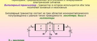
Transistor
In our amplifier we will use the simplest bipolar transistors. A transistor is made from a semiconductor material. The property we need of this material is the presence of free carriers of both positive and negative charges. Depending on which charges are greater, semiconductors are divided into two types according to conductivity: n
-type and
p
-type (n-negative, p-positive). Negative charges are electrons released from the outer shells of atoms in the crystal lattice, and positive charges are so-called holes. Holes are vacant spaces that remain in electron shells after electrons leave them. Conventionally, we denote atoms with an electron in the outer orbit by a blue circle with a minus sign, and atoms with a vacant place by an empty circle:
Each bipolar transistor consists of three zones of such semiconductors, these zones are called base, emitter and collector.
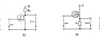
Let's look at an example of how a transistor works. To do this, connect two 1.5 and 5 volt batteries to the transistor, with the plus to the emitter and the minus to the base and collector, respectively (see figure):
An electromagnetic field will appear at the contact between the base and emitter, which literally pulls out electrons from the outer orbit of the base atoms and transfers them to the emitter. Free electrons leave behind holes and occupy vacant places already in the emitter. This same electromagnetic field has the same effect on the atoms of the collector, and since the base in the transistor is quite thin relative to the emitter and collector, the collector electrons quite easily pass through it to the emitter, and in much greater quantities than from the base.
If we turn off the voltage from the base, then there will be no electromagnetic field, and the base will act as a dielectric, and the transistor will be closed. Thus, by applying a sufficiently low voltage to the base, we can control the higher voltage applied to the emitter and collector.
The pnp transistor we reviewed
-type, since it has two
p
-zones and one
n
-zone.
There are also npn
transistors, the principle of operation in them is the same, but the electric current flows in them in the opposite direction than in the transistor we considered. This is how bipolar transistors are indicated on electrical diagrams, the arrow indicates the direction of the current:
ULF
Well, let's try to design a low-frequency amplifier from all this. First, we need a signal that we will amplify; it can be a computer sound card or any other audio device with a linear output. Let's say our signal with a maximum amplitude of approximately 0.5 volts at a current of 0.2 A, something like this:
And in order for the simplest 4-ohm 10-watt speaker to work, we need to increase the signal amplitude to 6 volts, with a current strength of I
=
U
/
R
= 6 / 4 = 1.5 A.
So, let's try to connect our signal to a transistor. Remember our circuit with a transistor and two batteries, now instead of a 1.5 volt battery we have a line output signal. Resistor R1 acts as a load so that there is no short circuit and our transistor does not burn out.
But here two problems arise at once, firstly our npn
-type, and opens only when the half-wave value is positive, and closes when the half-wave is negative.
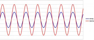
Secondly, a transistor, like any semiconductor device, has nonlinear characteristics in terms of voltage and current, and the lower the current and voltage values, the stronger these distortions:
Not only is there only a half-wave left of our signal, but it will also be distorted:
This is the so-called step-type distortion.
To get rid of these problems, we need to shift our signal to the working area of the transistor, where the entire sinusoid of the signal will fit and nonlinear distortions will be negligible. To do this, a bias voltage, say 1 volt, is applied to the base using a voltage divider made up of two resistors R2 and R3.
And our signal entering the transistor will look like this:
Now we need to remove our useful signal from the collector of the transistor. To do this, install capacitor C1:
As we remember, a capacitor allows alternating current to pass through and does not allow direct current to pass through, so it will serve as a filter that passes only our useful signal - our sine wave. And the constant component that has not passed through the capacitor will be dissipated by resistor R1. Alternating current, our useful signal, will tend to pass through the capacitor, so the resistance of the capacitor for it is negligible compared to resistor R1.
This is the first transistor stage of our amplifier. But there are two more small nuances:
We don’t know 100% what signal is entering the amplifier, what if the signal source is faulty, anything can happen, again static electricity or a constant voltage passes along with the useful signal. This may cause the transistor to not work properly or even cause it to break. To do this, we will install capacitor C2; like capacitor C1, it will block direct electric current, and the limited capacitance of the capacitor will not allow large amplitude peaks to pass through, which can damage the transistor. These power surges usually occur when the device is turned on or off.
And the second nuance is that any signal source requires a certain specific load (resistance). Therefore, the input impedance of the cascade is important for us. To adjust the input resistance, add resistor R4 to the emitter circuit:
Now we know the purpose of each resistor and capacitor in the transistor stage. Let's now try to calculate what element values need to be used for it.
Initial data:
- U
= 12 V - supply voltage; - U be
~ 1 V - Emitter-base voltage of the transistor operating point;
npn
transistor 2N2712 is suitable for us
- P max
= 200 mW - maximum power dissipation; - I max
= 100 mA - maximum constant collector current; - U max
= 18 V - maximum permissible collector-base / collector-emitter voltage (We have a supply voltage of 12 V, so there is enough to spare); - U eb
= 5 V - maximum permissible emitter-base voltage (our voltage is 1 volt ± 0.5 volt); - h21
= 75-225 - base current amplification factor, the minimum value is accepted - 75;
- We calculate the maximum static power of the transistor, it is taken 20% less than the maximum power dissipation, so that our transistor does not work at the limit of its capabilities:
P st.max= 0.8*
P max
= 0.8 * 200 mW = 160 mW; - Let's determine the collector current in static mode (without a signal), despite the fact that no voltage is supplied to the base through the transistor, electric current still flows to a small extent.
I k0=
P art.max
/
U ke
, where
U ke
is the voltage of the collector-emitter transition. Half of the supply voltage is dissipated on the transistor, the second half will be dissipated on resistors:U ke
=
U
/ 2;I k0
=
P art.max
/ (
U
/ 2) = 160 mW / (12V / 2) = 26.7 mA; - Now let's calculate the load resistance, initially we had one resistor R1, which performed this role, but since we added resistor R4 to increase the input resistance of the cascade, now the load resistance will be the sum of R1 and R4:
R n=
R1
+
R4
, where
Rn
is the total load resistance;The ratio between R1 and R4 is usually taken to be 1 to 10:
R1
=
R4
*10;Let's calculate the load resistance:
R1
+
R4
= (
U
/ 2) /
I k0
= (12V / 2) / 26.7 mA = (12V / 2) / 0.0267 A = 224.7 Ohm;The closest resistor values are 200 and 27 Ohms. R1
= 200 Ohm, and
R4
= 27 Ohm. - Now let’s find the voltage at the collector of the transistor without a signal:
U k0= (
U ke0
+
I k0
*
R4
) = (
U
-
I k0
*
R1
) = (12V -0.0267 A * 200 Ohm) = 6.7 V; - Transistor control base current:
I b=
I k
/
h21
, where
I k
is the collector current;I to
= (
U
/
Rn
);I b
= (
U
/
R n
) /
h21
= (12V / (200 Ohm + 27 Ohm)) / 75 = 0.0007 A = 0.07 mA; - The total base current is determined by the base bias voltage, which is set by the divider R2
And
R3
. The current specified by the divider should be 5-10 times greater than the base control current (
I b
), so that the base control current itself does not affect the bias voltage. Thus, for the current divider value (
I cases
) we accept 0.7 mA and calculate
R2
And
R3
:R2
+
R3
=
U
/
I div
= 12V / 0.007 = 1714.3 Ohm - Now let's calculate the voltage at the emitter at rest of the transistor (U e
):U e
=
I k0
*
R4
= 0.0267 A * 27 Ohm = 0.72 VYes, I k0
the collector's quiescent current, but the same current also passes through the emitter, so
I k0
is considered the quiescent current of the entire transistor. - We calculate the total voltage at the base (U b
) taking into account the bias voltage (
U cm
= 1V):U b
=
U e
+
U cm
= 0.72 + 1 = 1.72 VNow, using the voltage divider formula, we find the values of resistors R2
and
R3
:R3
= (
R2
+
R3
) *
U b
/
U
= 1714.3 Ohm * 1.72 V / 12 V = 245.7 Ohm;The closest resistor value is 250 ohms;
R2
= (
R2
+
R3
) -
R3
= 1714.3 Ohms - 250 Ohms = 1464.3 Ohms;We select the resistor value in the direction of decrease, the nearest R2
= 1.3 kOhm.
- Capacitors C1
and
C2
are usually set to at least 5 µF. The capacitance is chosen such that the capacitor does not have time to recharge.
Conclusion
At the output of the cascade, we receive a proportionally amplified signal in both current and voltage, that is, in power.
But one stage is not enough for us to achieve the required gain, so we will have to add the next and the next... And so on. The considered calculation is quite superficial and such an amplification circuit, of course, is not used in the construction of amplifiers; we must not forget about the range of transmitted frequencies, distortion and much more.
How to eat scheme
The quality of the amplification also depends on the quality of the power supply. No matter how outstanding the characteristics of the transistor, if the power supply is poorly filtered or insufficient, then the amplification will be of advisable quality.
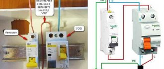
6 V power is connected to terminals X3 and X4.
This circuit can also be powered by a battery. However, despite the fact that the battery is a source with minimal noise, the battery also has its own resistance.
And so that it does not interfere or affect the operation of the amplifier, a smoothing and storage capacitor is needed.
Electrolytic capacitor C3 stores energy from the power supply, which improves the quality of amplification. The higher the capacity, the better. Naturally, this rule has limitations. If you install too large a container, there will be a large load on the power supply.
In addition, electrolytic capacitors must discharge after switching off. Moreover, there is a limit to increasing the capacity for the circuit. If a capacitor with a capacity of 1 farad (1,000,000 μF) is connected to this circuit, then the noise level at the amplifier output will be the same as at 1000 μF. This is due to the fact that the transistor also has its own “noise”, lack of shielding at the input, dynamic distortion and other parameters.
During circuit design, all these parameters are calculated. Here in the circuit, capacitor C3 has a capacity of 47 microfarads - this is enough for our transistor, since it does not have much power that it can produce. You can also supply a larger capacity, for example, 1000 microfarads. The main thing is not to carefully install a capacitor with a lower voltage limit. If you put a capacitor less than 6 V (power supply to the circuit), the capacitor will start to heat up and may even explode.
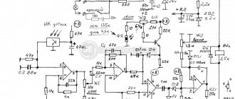
A simple DIY audio amplifier circuit
When creating a homemade device, a radio amateur has to solve many different problems. One of them is related to the output power, which is limited by the supply voltage. First of all, this applies to car systems, since they receive power from the on-board network. An exemplary option would be to use individual microcircuits. The circuit of a complete audio amplifier is a pre-stage with effective tone controls and a final block. The proposed design contains the following characteristics:
- Output power – 20 WX 2
- Frequency band – 40 – 18,000 Hz
- Distortion factor – 1.0%
- Supply voltage – 8-18 V
Sound amplifier for speakers printed circuit board diagram A powerful amplifier on a microcircuit assembled with your own hands can be used at home or installed in a car.
Amplifier input
The amplifier input is terminals X1 and X2.
X2 is the minus of the input, and X1 is the plus. Since the circuit is for one channel, the ULF is called mono.
You can connect both the left and right channels, or both at once.
Input filtering
Electrolytic capacitor C1 allows you to separate the DC component of the incoming signal from the variable one.
Simply put, it only passes the AC signal. If there is no signal, or the amplifier input is short-circuited, then without this capacitor the transistor may go into saturation mode (maximum gain), and an unpleasant wheeze will appear at the output.
Do not confuse this effect with whistling. The whistle is the influence of positive feedback, and in this case there will be a saturation mode due to a short circuit at the input. And at the output of the amplifier, it is the wheezing that will be heard, and not the sound or sound.
The capacitance of the capacitor is matched to the frequency of the sound signal. The sound starts from 20 Hz and up to 16 kHz.
Simple DIY sound amplifier
You can assemble an audio amplifier with your own hands without microcircuits using any transistors, including both bipolar and field-effect ones. The use of field-effect transistors in the output stage made it possible to create a device whose characteristics are close to those of tube designs.
The scheme has the following characteristics:
- The frequency response is linear in the range 20 Hz-100 kHz
- Distortion rate at 1 kHz does not exceed 0.003%
- Output power 10 watts into 8 ohm load
To drive the output stage, a voltage of 0.7 volts is required, which must be provided by the preliminary stage. The NE5534 operational amplifier can be replaced with the domestic op-amp KR140UD608. Zener diodes must be designed for a stabilization voltage of 18 volts. The 1N4705 can be replaced by two semiconductors in series, 9 volts each.
Operating point and base offset
To ensure that the transistor does not distort the input signal, you first need to open it slightly.
This can be done using a voltage divider consisting of two resistors R1 and R2. This voltage divider allows you to slightly open the transistor VT1 so that the input signal does not waste its electrical energy on its opening.
The current that flows through R1 and R2 goes to the base of transistor VT1, which then goes through the emitter, thereby opening it. This is called the base bias of the transistor, that is, its opening. The bias voltage determines the operating point. In this case, a class A amplifier.
How is the amplifier class determined?
The class of an amplifier is determined by its operating point. The operating point is selected using the current-voltage characteristic of the transistor. The higher the voltage applied to the transistor input, the greater the current, the higher the operating point.
For example, the point in the center is class A.
And the class is the highest quality of amplifiers. It amplifies both the positive and negative half-waves of the input signal. At the same time, this class has a significant drawback. This limits power and reduces energy efficiency. The fact is that as long as no input signal is received at the ULF input, it works all the time while it is turned on.
It turns out that this wastes excess electricity. Therefore, the operating point is also called the resting point, when the amplifier does not amplify the input signal.
The sensitivity of the amplifier also depends on the operating point.
There are also class B, AB and D. They differ from each other in amplification efficiency and the presence of distortion. It all depends on the scheme used.
For example. Class D does not open the transistor at all, but from the point of view of energy efficiency it is the best choice. The transistor does not consume anything at rest; it turns on only when an input signal is applied. And at the same time, if an analog audio signal is supplied to the input, it is distorted. Such a class will not be suitable for the scheme that we are analyzing in this article.
Therefore, circuit designers and engineers invented digital amplifiers. Their analog signal is converted to digital, and only then fed to the input of the amplifier. The transistor does not distort the signal with the input digit. After amplification, the signal is again converted to analog with the least loss and distortion.
And the AB mode is used in circuits where there are several transistors that operate at their own half-waves. There are circuits where one transistor amplifies only positive half-waves, and the second only negative ones. Such amplifiers are called push-pull.
Minuses
Having absolutely killer advantages, class D has not conquered the Hi-Fi market entirely only because it has its weaknesses, which for many connoisseurs of high-quality sound look much more significant than energy efficiency. The presence of a high-frequency generator in the circuit is itself a potential source of electromagnetic interference, which negatively affects the sound of the amplifier itself and the operation of the audio path components adjacent to it.
An untrained listener may not notice this effect or not attach any importance to it, but in the Hi-Fi and High End industry, when every little thing matters, such proximity is not welcome and forces engineers to improve filter circuits and go to other tricks to eliminate the influence malicious microwave carrier frequency generator to the reproduced audio signal.
The high efficiency of class D amplifiers is the reason for one specific feature: the high dependence of the quality and sound character on the power supply. If the manufacturer decides to use a switching power supply and does not bother with a sufficient number of filtering circuits, some of the noise will definitely penetrate the speakers and spoil the sound impression. A bad power supply, of course, will not benefit class AB, but it is in class D that this problem manifests itself most acutely.
Stabilization of the circuit operation
When a semiconductor heats up, its resistance decreases. The transistor is made of a semiconductor, and accordingly its pn junctions are too.
When the ULF circuit operates, current flows through the transistor and it heats up. Typically all power is dissipated at the collector. Nevertheless, the characteristics of the transistor change dramatically, since the resistance of its pn junction decreases sharply as the temperature rises.
To stabilize the operation of the transistor, you need to balance its resistance with another source. This can be done using additional resistance.
When the resistance of transistor VT1 decreases, resistor R3 takes part of the voltage onto itself and does not allow the current in the circuit to increase.
Thanks to this, the transistor:
- does not close;
- does not go into saturation mode;
- does not distort the signal;
- and doesn't overheat.
This is called thermal stabilization of the amplifier.
And so that in normal operation, when VT1 does not heat up, resistor R3 does not reduce the power of the circuit, a shunt electrolytic capacitor C2 is included in the circuit. The variable component of the input signal passes through it without loss.
What else to look for when choosing an amplifier
Let's consider what points you should pay attention to in order to choose a sound amplifier with the optimal ratio of functionality, price and quality.
- Device cost. The low cost should alert you. You should not buy inexpensive devices.
- The area of the room where the amplifier will be installed. This affects the sound quality. It should be taken into account that the power per channel is 3-5 watts per square meter. If the parameters do not exceed fifteen square meters, then the first figure must be taken into account; for areas greater than twenty square meters - the second.
- Buy devices from companies and stores where it is possible to check the quality of the device in action.
- It is necessary to select equipment with a power reserve, since the devices should not be used at maximum power. All this can affect the service life of the device. The most reliable amplifiers are considered to have a power of up to one hundred watts.
- If possible, you should choose equipment from the same manufacturer. In cases where this is not possible, try to choose a device of the same class.
Amplifier output
At the output of the amplifier, you can connect either another amplifier, which will amplify the signal even more, or a dynamic head. The dynamic head is a regular speaker. It will reproduce the sound from the output of transistor VT1.
However, there are many nuances here too.
The most important thing concerns the matching of the load resistance and the amplifier resistance.
If the output resistance of the transistor is much greater than that of the dynamic head, then it will not be able to transmit all the power. At a minimum, most of the voltage will remain on its contacts.
This circuit requires a speaker with a resistance of about 1 kOhm.
If you set it less, for example, by 4 Ohms, then even half the power will not be reproduced, and the VT1 collector will begin to heat up even more.
The matching of the input, output and amplifier load resistances is calculated at the circuit design stage. Therefore, they should not be violated.
Practice
The honorable duty of defending the honor of class D amplifiers in our study fell to the Marantz PM-KI RUBY amplifier. This device has an exemplary layout that demonstrates how modern amplifiers should be created. Two Hypex NCore 500 modules operating in class D are powered by a special low-noise switching power supply. At the same time, the design of the amplifier contains a classic preliminary stage, built on discrete elements, according to Marantz’s proprietary HDAM technology, which was also used in traditional class AB amplifiers.
The preliminary stage is powered by a linear power supply, the toroidal transformer of which, judging by its size, has a multiple power reserve so as not to in any way affect the dynamics and purity of sound. In other words, two approaches are combined in one housing: a classic one for a preamplifier and a modern one for a power amplifier.
All this is richly seasoned with the typical attention to detail for High-End models, such as a copper-plated chassis, improved vibration isolation, shorter signal paths, symmetrical board topology, strict selection of parts according to parameters, etc.
As a result, we have perhaps the most advanced device from a technical point of view with a damping factor of 500, distortion of less than 0.005% and power consumption of 130 W with an output power of up to 200 W per channel at 4 Ohm load. However, any claim to perfection in the world of sound must be verified by practice.
How does current flow through the circuit?
At the initial moment of time, when the power is connected, the electrolytic capacitor C3 is charged, and the collector and emitter of the transistor VT1 begin to be powered. And also the current passes through the voltage divider.
The voltage divider R1, R2 biases the base of VT1. The base-emitter bias current (B-E) begins to flow, thereby establishing the ULF operating point.
When the input signal arrives at terminal X1, it passes through C1 and through the divider enters the base of VT1 and partially leaves through the emitter.
The input signal is attracted by the collector VT1 and thereby amplified.
That part of the alternating signal that has passed to the emitter of the transistor is amplified by the emitter current. It passes freely through C2, which, paired with R3, stabilizes the amplifier’s operating mode from overheating and distortion. As a result, the input signal, amplified by the collector-emitter (C-E) current VT1, is sent to the output, that is, to the dynamic head BF1.
What determines the power of the circuit?
This scheme has limitations. You can change VT1 KT315 to a more powerful one, which will have a higher gain, but this gain limit is not infinite.
First of all, it all depends on the transistor used. If you change it to a more powerful one, then the gain will be higher. But it should be remembered that the more powerful the transistor, the more powerful the input signal is needed. In addition, you will have to recalculate all components. And connect the preamplifier, assemble the power supply circuit, and this will be a completely different circuit.
Transistors have a number of parameters that affect the circuit. This is the gain for current (h21e), voltage, power. Another important parameter is the power dissipation on the collector. As power increases, a radiator will be required to remove heat.
Peculiarities
Descriptions of the pros and cons of class D circuitry give absolutely unambiguous hints about what developers who strive to achieve maximum quality sound from amplifiers should primarily do.
Developers solve the problem of powering class D amplifiers in two ways. Some follow the proven path, using classic linear power supplies with huge toroidal transformers and other classic solutions. But there is another path that a minority of developers take. With the right skill, it is quite possible to create a low-noise switching power supply suitable for installation in amplifiers of the highest quality class. And it is they that are able to give a head start to the most powerful and reputable linear power supplies due to better efficiency and performance, and as a result, better sound dynamics and instant response of the amplifier to large differences in signal levels.
As for the specifics of the operation of the class D amplifier itself, its circuit design provides a significantly higher damping coefficient in comparison with class AB and other circuit solutions. This guarantees not only stable operation with complex loads, fast, clear bass and a large dynamic range, but also ensures lower levels of distortion, the absence of muss, sluggish attack or blurred fronts and, most importantly, the ability of the amplifier to equally cope with completely diverse music.
How to assemble a circuit
The circuit can be assembled on a PCB or on a breadboard. Follow the link to this article, it describes in more detail the process of assembling and testing the circuit.
Use quality parts and good solder. She's working. This is generally a classic circuit for connecting a bipolar transistor with a common emitter.
Also on the site there are other amplifier circuits that are not difficult to assemble and not expensive in terms of the cost of parts.
Audio amplifier for speakers circuit board circuit
The printed circuit board for this circuit is made of foil-coated PCB by etching. The pattern of printed tracks can be applied with asphalt-bitumen varnish or other composition. The easiest way to etch a board is in a ferric chloride solution. In order for the audio amplifier on a microcircuit, made by yourself, to work stably, we install the TDA1552Q element on the radiator. To obtain good sound and minimal distortion, capacitors C11, 12, 13 and 14 must be film. Resistors R7 and R8 set the maximum undistorted signal on the speaker systems.