The scope of application of diodes is not limited to rectifiers. In fact, this area is very broad. Among other things, diodes are used for protective purposes. For example, to protect electronic devices when they are mistakenly switched on with the wrong polarity, to protect the inputs of various circuits from overload, to prevent breakdowns of semiconductor switches from self-induction EMF pulses that occur when inductive loads are disconnected, etc.
In order to protect the inputs of digital and analog microcircuits from voltage overloads, chains of two diodes are used, which are connected in the opposite direction to the power buses of the microcircuit, and the middle point of the diode chain is connected to the protected input.
If a normal voltage is supplied to the input of the circuit, then the diodes remain in a closed state and have almost no effect on the operation of the microcircuit and the circuit as a whole.
But as soon as the potential of the protected input goes beyond the supply voltage, one of the diodes will go into a conducting state and begin to bypass this input, thus limiting the allowed input potential to the value of the supply voltage plus the direct voltage drop across the diode.
Chains of this kind are sometimes immediately included in an integrated circuit at the stage of designing its crystal, or are put into the circuit later, at the stage of developing a node, block or entire device. Protective two-diode assemblies are also produced in the form of finished microelectronic components in three-terminal transistor packages.
If the protective voltage range needs to be expanded, then instead of connecting to buses with supply potentials, the diodes are connected to points with other potentials that will provide the required permitted range.
On long wire lines, sometimes powerful interference occurs, for example from lightning discharges. To protect against them, more complex circuits may be required, containing not only two diodes, but also resistors, arresters, capacitors and varistors.
As is known, it is the EMF of self-induction that prevents the decrease in current through any inductance, trying to somehow maintain the current through it unchanged. But at the moment when the current source from the coil is turned off, the magnetic field of the inductance must dissipate its energy somewhere, the value of which is equal to
So, as soon as the inductance is turned off, it itself turns into a source of voltage and current, and at that moment a voltage appears on the private key, the value of which can be dangerous for the key. For semiconductor switches, this is fraught with breakdown of the switch itself, because the energy will quickly and with very high power be dissipated on the switch. For mechanical switches, the consequences may be sparking and burning of contacts.
Due to its simplicity, diode protection is very widespread and allows you to protect various switches that interact with an inductive load.
To protect a switch with an inductive load, a diode is connected in parallel with the coil in such a direction that when operating current initially flows through the coil, the diode is blocked. But as soon as the current in the coil is turned off, a self-inductive emf arises, which has a polarity opposite to the voltage previously applied to the inductance.
This self-induction EMF unlocks the diode, and now the current, which at the previous moment was directed through the inductance, moves through the diode, and the energy of the magnetic field is dissipated on the diode or on the snubber circuit in which it is connected. This way the switch will not be damaged by excessive voltage applied to its electrodes.
When the protective circuit includes only one diode, the voltage across the coil will be equal to the forward voltage drop across the diode, that is, in the region of 0.7 to 1.2 volts, depending on the magnitude of the current.
But since the voltage on the diode in this case is low, the current will decrease slowly, and in order to speed up the load shutdown, it may be necessary to use a more complex protective circuit, including not only a diode, but also in series with the diode - a zener diode, or a diode with a resistor or varistor - a full-fledged snubber chain.
If you liked this article, share a link to it on social networks. This will greatly help the development of our site!
Source
Protective diode (suppressor): operating principle, how to test a TVS diode.
The protection diode is a guest of our review of semiconductors.
The power of interference affecting the voltage level in the device may vary. To counter high-energy pulses, it is possible to use gas dischargers and protective thyristors. To protect yourself from medium and low-power influences, protective diodes and varistors are more suitable.
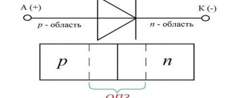
Protection diode , most often made of silicon, may be called:
Often the suppressor becomes one of the components of the switching power supply unit, since in the event of a malfunction of the unit, the suppressor can protect it from overvoltage. Initially, the protective diode was created as insurance against atmospheric electrical influences on devices.
There are several areas of modern application of limiting zener diodes:
How to choose the right suppressor
In order not to make a mistake in choosing this device, you should follow simple recommendations:
- set the rated voltage level on the line;
- determine exactly how the element will be installed;
- determine the type of voltage, and also establish that the reverse voltage exceeds the rated voltage of the circuit;
- identify acceptable operating temperature limits;
- decide what type of diode is required (symmetrical or asymmetrical);
- decide on the most suitable series and product option.
In addition, before purchasing, it is recommended to additionally make sure that the dimensions and parameters of the radio element comply with the requirements and installation nuances.
The use of modern protective diodes in circuits is highly effective in protecting any electrical equipment connected to overhead lines.
Operating principles
The protective diode has a specific VA characteristic characterized by nonlinearity. Provided that the size of the pulse amplitude is greater than permissible, this will entail a so-called “avalanche breakdown”. In other words, the amplitude size will be normalized, and all excess will be removed from the network through a protective diode.
Fig. 1 Protective diode - principle of operation of a semiconductor
The operating principle of a TVS diode assumes that until a danger occurs, the diode fuse in no way affects the device itself or its functional properties. Thus, it should be noted that another name for the protective diode is emerging - an avalanche diode.
There are two types of limiting zener diodes:
Protective diode, bidirectional, suitable for operation in alternating current networks.
Applicable only for networks with direct current, since they have a unidirectional operating mode. The method of connecting an asymmetrical protective diode does not correspond to the standard. Its anode is connected to the negative bus, and its cathode is connected to the positive bus. The position turns out to be conditionally inverted.
The coding of protective diodes classified as symmetrical includes the letters “ C ” or “ CA ”. Single-ended diode fuses have a color-coded stripe on the cathode terminal side.
The housing of each protective diode is also equipped with a marking code that displays all significant parameters in a compressed form.
If the input voltage level of the diode increases, the zener diode will reduce its internal resistance over a very short period of time. The current strength at this moment, on the contrary, will increase, and the fuse will blow. Since the protective diode almost instantly, the integrity of the main circuit is not compromised. In fact, a quick response to excess voltage is the most important advantage of a TVS diode .
Types and designation
There are two main types of TVS protection diodes:
- symmetrical (bidirectional) - actively used in circuits with bipolar voltage, which allows their use in alternating current networks;
- asymmetrical (unidirectional) - effectively protect circuits with voltage of the same polarity, which allows their use in DC networks.
In the diagrams, suppressors are designated as VD1, VD2 (bidirectional) and VD3 (asymmetrical). The rated voltage of such diode fuses varies from 6.8 to 440 volts. And the operating temperature ranges from -65 to +175 degrees Celsius. High response speed reliably protects equipment from overvoltage. The diode fuse housing is equipped with a marking code that displays all the important parameters of the product.
The marking of protective diodes allows you to select the most suitable radio element for DC or AC networks. Asymmetrical products have a colored marking ring on the body. Numbers and letters usually indicate power, breakdown voltage, and permissible voltage deviation.
Significant characteristics of protection diodes
The voltage value at which the diode opens and the potential is transferred to the common wire. An additional synonymous designation is VBR.
Maximum reverse leakage current. It has a small value, measured in microamps, and the functionality of the device practically does not depend on it. Additional designation - IR.
The value is an indicator of constant reverse voltage. V.R.W.M.
The highest value for limiting impulse voltage. VCL, VCmax.
The highest value of the peak pulse current. Otherwise, this is an indicator of the greatest strength of the current pulse that is safe for the protective diode. For the most effective limiting zener diodes, this value can be hundreds of amperes. IPP.
Indicator of the highest value of permissible pulse power. Unfortunately, this parameter is extremely dependent on the pulse duration.
Fig. 2 VA characteristics of the protective diode
The power level of protection diodes is not the same. However, if the suppressor does not have enough initial data on this parameter, it can easily be combined with one or more semiconductors, which will have a positive effect on the overall power level.
A TVS diode can act as a zener diode. But first you need to check its maximum power dissipation and dynamic current at Imax. and Imin.
Introduction
Any highly reliable industrial electronic equipment designed using semiconductor devices (microprocessors, digital and analog ICs) requires electrical overload protection circuits.
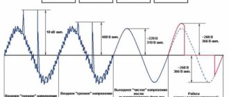
Overloads have a different nature and differ in power level; the most dangerous among them are voltage drops, which are random ripples with amplitudes greater than the operating voltages in the circuit. They arise as a result of exposure to short-term electromagnetic pulses of natural (powerful lightning discharges) or artificial (radiation from radio transmitting devices, high-voltage transmission lines) origin, as well as due to internal transient processes caused by switching capacitive or inductive loads (electric motors, generators) and electrostatic discharges ( ESD). The influence of electromagnetic pulses of any origin leads to changes in the parameters of electronic components both due to the direct absorption of energy and due to the impact on them of voltage and current pulses induced in the electrical circuits of the equipment. The most common causes of overvoltage are lightning and static discharges.
To test electrical equipment for resistance to these factors, IEC 61000 is used, the currently most recognized international standard that defines refined parameters of test signals. Their characteristics were obtained through numerous measurements using generally accepted monitoring methods. In Fig. 1 shows typical pulse shapes corresponding to lightning (IEC 61000-4-5 standard) and electrostatic (IEC 61000-4-2) discharges.
Rice. 1. Characteristics of current pulses caused by: a) lightning discharge; b) electrostatic discharge
Lightning discharges are characterized by high-energy pulses with durations ranging from several tens to thousands of microseconds and very high currents (tens of kiloamperes). A direct lightning strike is a destructive but rare occurrence. Much more often, harm is caused by the magnetic field created during a discharge, which generates interference pulses in nearby electrical objects (electrical cables of transmission lines, etc.). Thus, cloud-to-cloud lightning can cause a stray voltage with an amplitude of up to 70 V in an electric cable located at a distance of 1.6 km from the source [1].
The human body is an excellent static voltage accumulator. During active activity, a static charge accumulates on the human body, and a discharge occurs upon contact with a conductive object. Also, network wires are capable of accumulating potential during operation; in this case, electrostatic discharge occurs when the cable is connected to the connector. The amplitude of electrostatic discharges can reach 35 kV, the excited signal has a rise time of about 1 ns. Although the energy released by driving such a pulse is small, the extremely short rise time and large peak voltage surge can cause catastrophic destruction of discrete semiconductor and integrated circuit devices. For example, in MOS structures, a point breakdown of the oxide layer and, accordingly, a deterioration in its dielectric strength leads to overheating and destruction of the gate even with low power dissipation. This, in turn, shortens the life of electronic equipment or completely destroys it.
Modern digital and analog ICs themselves typically have special protection circuits that provide conductive paths to eliminate interference. However, they are not able to handle large currents. In addition, given the current trend toward miniaturization, it is difficult to achieve sufficient levels of protection using on-chip circuits alone, as they must be sacrificed in order to improve key performance characteristics and reduce power consumption. According to the forecasts of the EOS/ESD association, in the future, ICs will not contain circuits that limit ESD pulses with an amplitude above 2 kV [2]. Therefore, to meet the requirements of IEC 61000 and bring competitive products to market, external protection must be designed and implemented in addition to the integrated one.
There are many devices on the market that provide good surge protection, but to select the most effective ones for a particular application, you need to carefully compare their parameters taking into account the operating conditions of the system. In addition to traditional fuses and simple LC and RC filters, specialized devices are widely used - gas arresters, metal oxide varistors and TVS diodes (Transient Voltage Suppression), also called suppressors, protective diodes and semiconductor voltage limiters in various sources. Each of the listed protective elements has advantages and disadvantages (Table 1).
Table 1. Comparison of parameters of specialized surge protection devices
| Parameter | Gas arresters | Varistors | TVS diodes |
| Pulse current level | High | High | Average |
| Turn-on voltage accuracy | Low | Low | High |
| Own capacity | Small | Big | Small |
| Life time | Small | Limited | Big |
| Performance | Low | Low | High |
| Price | High | Average | Low |
Gas arresters are used to protect equipment from the most powerful interference, they are used as the primary protection of telecommunications and power circuits. The value of their peak currents reaches thousands of amperes, and the number of operations turns out to be quite large. Disadvantages include high switching voltage, large dimensions and low performance. Long response times (more than 0.15 μs) do not solve the problem of protecting many semiconductor devices and microcircuits.
Varistors, due to the high ratio of peak currents and dimensions, are optimal for creating the most compact solutions while protecting against powerful interference. With a wide range of operating currents and voltages, they successfully serve to protect electronic components on printed circuit boards, one of the main applications being automotive electronics. Disadvantages include limited service life and large intrinsic capacitance (thousands of picofarads), which prevents their inclusion in high-speed data lines.
TVS diodes, which have the lowest clamping voltages and the fastest response times of all the listed components, can be used in low-voltage circuits. They are well suited for the protection of semiconductor devices or for providing the final stage in combined protective devices. Other obvious advantages include high durability and reliability, a wide range of operating voltages, and the ability to obtain compact multi-channel solutions in planar mounting packages. Low intrinsic capacitance, which does not affect signal and logic lines, allows them to be installed in various communication interfaces.
Checking the integrity of the protective diode
Checking the integrity of the protective, as well as the rectifying (including power) diode, is carried out with a multimeter (as an option, you can use an ohmmeter). The device can be used for this purpose only in dialing mode.
Fig 3 Checking the protective diode
When the multimeter is ready, you need to connect it with probes to the suppressor terminals (positive-red with the anode, negative-black with the cathode). When this is done, the display of the testing device will display a number indicating the threshold voltage of the diode fuse being tested. When changing the polarity of the connection, an infinite resistance value should be displayed. If everything turned out this way, then the element is working.
If a leak is detected during a pole change, we can talk about the dysfunction of the element and the need to replace it. Similarly, you can check the protective diode of a car generator.
Basic qualities of TVS diodes
But, as a result, it is necessary to recognize that the fulfillment of one condition often entails a violation of another.
In addition, the TVS diode, in principle, cannot be considered an ideal protective limiter. For example, suppressor protective diodes in the “off” position can be characterized by fairly large reverse currents. Further, abruptness when changing modes is disapproved. The biggest problem is that in the limiting mode the voltage level is directly dependent on the current strength.
It must be remembered that all diode characteristics given by the manufacturer are valid only under specific temperature conditions. At higher temperatures, the permissible peak power and currents will decrease.
However, even despite such shortcomings, diode fuses still turn out to be better than instruments, devices and elements with a similar purpose.
TVS diode: purpose of the device + technical characteristics
In fact, the purpose of a TVS diode installed at the input of an electrical circuit is to have a minimum influence on the process at moments of nominal operation. Only under transient overvoltage conditions will the device immediately conduct and shunt current to ground, thereby maintaining the circuit voltage at a safe low level.
Connection diagram showing how the protection functions, which to some extent determines how to choose a TVS diode: 1 - input/output source; 2 — direction of pulse current; 3 - protective TVS diode; 4 - integrated circuit protected from overvoltage
In fact, TVS diodes do not have ideal characteristics at all, which must be taken into account to ensure reliable protection and minimal impact on the electrical circuit. The lack of ideality factor is somewhat comparable to ESD diodes. However, since surge protection diodes are more important to the reliability of the electrical circuit, these devices require additional consideration during selection.
Designation, parameters and application of protective diodes
Among the variety of semiconductor devices, diodes are probably the largest family. Schottky diodes, Gunn diodes, zener diodes, LEDs, photodiodes, tunnel diodes and many more different types and applications.
One of the classes of semiconductor diodes in our literature is called SOL (semiconductor voltage limiter) or suppressor. In foreign technical literature the name TVS diode ( Transient Voltage Suppressor is . Very often, TVS diodes are named by manufacturer brands: TRANSIL, INSEL.
In the technical literature and among radio amateurs, a suppressor can be called differently: protective diode, limiting zener diode, TVS diode, transil, voltage limiter, limiting diode. Suppressors can often be found in switching power supplies - there they serve as protection against overvoltage of the powered circuit in the event of faults in the switching power supply.
Let's consider what a TVS diode is, its principle of operation, in what circuits and for what purposes it is used.
TVS diodes were created in 1968 in the USA to protect industrial equipment from atmospheric electricity discharges. In the operating conditions of electronic devices for both industrial and household purposes, great importance is attached to protecting these devices from natural electrical impulses.
Voltage surges also often occur at power transformer substations. In such cases, hundreds of household appliances break down. Because industrial enterprises have comprehensive protection, but residential buildings are not protected at all in this case.
To protect equipment from the effects of electrical overvoltages, a class of semiconductor devices called TVS diodes or “suppressors” was developed. Sometimes in a conversation you can hear: diode fuse.
Designation on the diagram.
Operating principle of a suppressor (protective diode).
TVS diodes have a pronounced nonlinear current-voltage characteristic. If the amplitude of the electrical pulse exceeds the rated voltage for a particular type of diode, it will go into avalanche breakdown mode. That is, the TVS diode will limit the voltage pulse to a normal value, and the “excess” goes to the case (ground) through the diode. The process looks more clearly in the figure.
As long as there is no threat of failure of the electronic device, the TVS diode does not have any effect on the operation of the equipment. This semiconductor device is faster than previous limiters.
Safety diodes are available both asymmetrical (unidirectional) and symmetrical (bidirectional). Symmetrical ones can operate in circuits with bipolar voltages, and asymmetrical ones only with voltages of one polarity. Another typical connection diagram (for a bidirectional diode).
For a unidirectional suppressor, the circuit looks a little different.
If the input voltage increases, the device reduces its resistance in a very short time. The current in the circuit increases sharply and the fuse blows. Since the suppressor operates very quickly, there is no harm to the equipment. A distinctive feature of TVS diodes is their very short response time to overvoltage. This is one of the “features” of protective diodes.
Basic electrical parameters of suppressors.
U samples (V) – breakdown voltage value. In foreign technical documentation, this parameter is designated as VBR ( Breakdown Voltage ). This is the voltage value at which the diode suddenly opens and diverts a dangerous current pulse to the common wire (“to ground”).
I arr. (µA) – value of constant reverse current. This is the value of the maximum reverse leakage current that all diodes have. It is very small and has virtually no effect on the operation of the circuit. Another designation is IR ( Max. Reverse Leakage Current ). May also be referred to as IRM.
U arr. (V) – constant reverse voltage. Corresponds to the English abbreviation VRWM ( Working Peak Reverse Voltage ). May be referred to as VRM.
U limit imp. (V) – maximum impulse limiting voltage. In datasheets it is designated as VCL or VC – Max. Clamping Voltage or simply Clamping Voltage .
I ogr. max. (A) – maximum peak pulse current. In English it is designated as IPP ( Max. Peak Pulse Current ). This value shows the maximum value of the current pulse the suppressor can withstand without destruction. For powerful suppressors, this value can reach several hundred amperes!
P imp. (Watt) – maximum permissible pulse power. This parameter shows how much power the suppressor can suppress. Let us recall that the word suppressor comes from the English word Suppressor , which means “suppressor”. Foreign name for the parameter Peak Pulse Power ( PPP ).
The value of the maximum pulse power can be found by multiplying the values of U limit. imp. ( VCL ) and I limit. max. ( IPP ).
The current-voltage characteristics of a symmetrical and asymmetrical TVS diode are as follows.
CVC of a unidirectional protective diode (suppressor) CVC of a bidirectional suppressor
The big disadvantage of these diodes is the large dependence of the maximum pulse power on the pulse duration. Typically, the operation of a TVS diode is considered when a pulse is applied to it with a minimum rise time of about 10 microseconds and a short duration.
For example, with a pulse duration of 50 microseconds, an SMBJ 12A diode can withstand a pulse current that is almost four times the rated one.
Small-sized diodes TRANSZORB TM series 1.5KE6.8 - 1.5KE440 (C)A . They are available in both symmetrical and asymmetrical versions. For a symmetrical diode, the letter C or CA is added to the designation. This series has a wide range of operating voltages from 5.0 to 376 volts, a short response time of 1 * 10-9 sec, and the ability to suppress high-power pulses up to 1500 W. They have proven themselves excellent in protection schemes for television, digital and other modern equipment.
Diodes are available in DO-201 package.
Dimensions are indicated in inches and millimeters (in parentheses). Asymmetrical suppressors have a colored marking ring on the body, which is located closer to the cathode terminal.
The body contains the marking of the protective diode, which encodes its main parameters.
Bidirectional diodes TRANSIL TM 1.5KE440CA are successfully used to protect household electronic equipment in 220 volt networks. Their use is most effective for protecting objects that are connected to overhead lines. In this case, there will be protection both from atmospheric electrical impulses and from impulse overvoltages along power circuits.
Source
TVS diodes TRANSZORB from General Semiconductor
TRANSZORB TVS diodes from General Semiconductor are available in various designs, taking into account operating conditions and areas of application. Discrete diodes in a plastic case with flexible leads designed for installation in through holes are available with maximum permissible pulse power values of 400 W, 500 W, 600 W, 1.5 kW and 5 kW. Diodes with the highest values of the maximum permissible pulse power are usually used for installation in power circuits. At lower power levels, high-density applications use diodes and diode assemblies that are available in both DIP and surface mount packages. They are available with maximum permissible pulse power values of 400 W, 500 W, 600 W, 1.5 kW and 5 kW. Diode assemblies are commonly used on data lines to protect I/O ports from ESD. In addition, specialized low-capacitance TVS diodes are produced, used in circuits with high data rates to prevent attenuation of useful signals. TRANSZORB TVS diodes are available for operation in circuits with operating voltages from 5 to 376 V. Due to the wide range of possible operating voltages and permissible power ratings (as well as overvoltages), TRANSZORB TVS diodes are used in a variety of electronic circuits and applications.
Topic: Are protection diodes needed?
Theme Options
In some PA circuits there are diodes between the output and the power buses (of course, in reverse connection), protecting the output transistors from reverse polarity voltage. They are used, for example, in the following amplifiers: “Brig”, Kletsov (83), Zuev (84), Gumelya (85). Most schemes, especially modern ones, do not have them. Meanwhile, I am not aware of cases of failure of transistors in PAs without these diodes. So are they needed? More precisely, is it necessary to protect modern high-power high-voltage transistors with them?
Diodes may be needed if the amplifier protection operates on the principle of sharp current cutoff. Then, when it is triggered, a situation is possible when a large current in the inductive load is applied to the output of the amplifier.
Power field-effect transistors have this diode in the transistor structure itself. They should be installed with bioplar ones if the circuit has a limitation of the output signal from the repeater. If the driver limits and the residual voltage on the transistor is more than 5 V, then this diode will not protect anything and the protection must be done differently.
In a state of avalanche breakdown, there will usually be 7-8 V at the emitter junction. How dangerous this is for the transistor depends on the current. Based on the fact that the area of the emitter junction is smaller than the collector junction, and the dissipation of high power on it will cause local heating of the crystal, up to 2-3 A is safe, 5-6 is critical and more than 8 is fatal, if we talk about powerful modern transistors with a permissible collector current 15A. The base current has no effect here, since nothing will flow through the base electrode.
Source
Basic diode faults
Sometimes devices of this type fail, this may occur due to natural depreciation and aging of these elements or for other reasons.
In total, there are 3 main types of common faults:
- Breakdown of the junction leads to the fact that the diode, instead of a semiconductor device, becomes essentially a very ordinary conductor. In this state, it loses its basic properties and begins to pass electric current in absolutely any direction. Such a breakdown is easily detected using a standard multimeter, which starts beeping and shows a low resistance level in the diode.
- When a break occurs, the reverse process occurs - the device generally stops passing electric current in any direction, that is, it essentially becomes an insulator. To accurately determine a break, it is necessary to use testers with high-quality and serviceable probes, otherwise they can sometimes falsely diagnose this malfunction. In alloy semiconductor varieties, such a breakdown is extremely rare.
- A leak during which the seal of the device body is broken, as a result of which it cannot function properly.
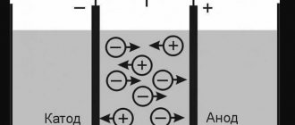
Breakdown of pn junction
Such breakdowns occur in situations where the reverse electric current begins to suddenly and sharply increase, this happens due to the fact that the voltage of the corresponding type reaches unacceptable high values.
There are usually several types:
- Thermal breakdowns, which are caused by a sharp increase in temperature and subsequent overheating.
- Electrical breakdowns that occur under the influence of current on the junction.
The graph of the current-voltage characteristic allows you to visually study these processes and the difference between them.
Electrical breakdown
The consequences caused by electrical breakdowns are not irreversible, since they do not destroy the crystal itself. Therefore, with a gradual decrease in voltage, it is possible to restore all the properties and operating parameters of the diode.
At the same time, breakdowns of this type are divided into two types:
- Tunneling breakdowns occur when high voltage passes through narrow junctions, which allows individual electrons to escape through it. They usually occur if semiconductor molecules contain a large number of different impurities. During such a breakdown, the reverse current begins to increase sharply and rapidly, and the corresponding voltage is at a low level.
- Avalanche types of breakdowns are possible due to the influence of strong fields that can accelerate charge carriers to the maximum level, due to which they knock out a number of valence electrons from atoms, which then fly into the conductive region. This phenomenon is avalanche-like in nature, which is why this type of breakdown received its name.
Thermal breakdown
The occurrence of such a breakdown can occur for two main reasons: insufficient heat removal and overheating of the pn junction, which occurs due to the flow of electric current through it at too high rates.
An increase in temperature in the transition and neighboring areas causes the following consequences:
- The growth of vibrations of the atoms that make up the crystal.
- Electrons entering the conductive band.
- A sharp increase in temperature.
- Destruction and deformation of the crystal structure.
- Complete failure and breakdown of the entire radio component.
Protective diodes operating principle
The protection diode is a guest of our review of semiconductors.
The power of interference affecting the voltage level in the device may vary. To counter high-energy pulses, it is possible to use gas dischargers and protective thyristors. To protect yourself from medium and low-power influences, protective diodes and varistors are more suitable.
Protection diode , most often made of silicon, may be called:
Often the suppressor becomes one of the components of the switching power supply unit, since in the event of a malfunction of the unit, the suppressor can protect it from overvoltage. Initially, the protective diode was created as insurance against atmospheric electrical influences on devices.
There are several areas of modern application of limiting zener diodes:
Application areas of diodes
Such radioelements are actively used in various directions:
- communications and telecommunications;
- digital interfaces;
- various power electronics;
- household electrical appliances;
- various control schemes.
Avalanche diodes are widely used to protect on-board electronics of vehicles. For example, the ignition system of any car is one of the most powerful sources of electrical impulses. Domestic protective diodes (Kremniy, SZTP, Foton, STC SIT, Saransk, TOR, Russia and others) are not inferior in quality, efficiency and availability to foreign analogues.
Operating principles
The protective diode has a specific VA characteristic characterized by nonlinearity. Provided that the size of the pulse amplitude is greater than permissible, this will entail a so-called “avalanche breakdown”. In other words, the amplitude size will be normalized, and all excess will be removed from the network through a protective diode.
Fig. 1 Protective diode - principle of operation of a semiconductor
The operating principle of a TVS diode assumes that until a danger occurs, the diode fuse in no way affects the device itself or its functional properties. Thus, it should be noted that another name for the protective diode is emerging - an avalanche diode.
There are two types of limiting zener diodes:
Protective diode, bidirectional, suitable for operation in alternating current networks.
Applicable only for networks with direct current, since they have a unidirectional operating mode. The method of connecting an asymmetrical protective diode does not correspond to the standard. Its anode is connected to the negative bus, and its cathode is connected to the positive bus. The position turns out to be conditionally inverted.
The coding of protective diodes classified as symmetrical includes the letters “ C ” or “ CA ”. Single-ended diode fuses have a color-coded stripe on the cathode terminal side.
The housing of each protective diode is also equipped with a marking code that displays all significant parameters in a compressed form.
If the input voltage level of the diode increases, the zener diode will reduce its internal resistance over a very short period of time. The current strength at this moment, on the contrary, will increase, and the fuse will blow. Since the protective diode almost instantly, the integrity of the main circuit is not compromised. In fact, a quick response to excess voltage is the most important advantage of a TVS diode .
TVS products Semtech Corporation
Semtech's protective products include both discrete diodes and specialized assemblies designed to work with specific interfaces [3]. This class of devices was designed to protect sensitive components from electrostatic discharge (ESD), electrical fast transients (EFT), and communications surge (CDE). Currently produced devices are available in a variety of housing designs, determined by operating conditions and areas of application, all products are certified to comply with the requirements of IEC, ETSI, Bellcore 1089 and FCC Part 68 safety standards and regulations. Typical applications include portable wearable electronics, equipment Ethernet and other data networks, HD TVs and monitors, laptops, personal and tablet computers.
The range of TVS devices offered by the company contains hundreds of items grouped into separate families; it is not possible to list their parameters in one article. Therefore, further we will consider the most interesting series from the point of view of competitive advantages, which include:
- low limiting voltage (from 2.5 V);
- high overload capacity;
- low intrinsic capacitance (less than 0.5 pF);
- the ability to protect against periodically repeating ESD pulses;
- minimum dimensions;
- low leakage currents.
Rice. 3. Internal structure of protective devices of the EMIClamp series: a) EClamp237xK; b) EClamp2422N; c) EClamp239xP
A series of protective devices that combine TVS diodes and LC/RC filters in single packages is produced by Semtech under the EMIClamp brand.
In addition to limiting spurious ESD pulses, it provides suppression of unwanted electromagnetic (EMI) and radio frequency (RFI) emissions in the frequency ranges determined by the parameters of the built-in low-pass filters. Components in this series protect common interfaces and are successfully used in portable electronics: cell phones, digital photo and video cameras, tablets and laptops, PC peripherals (printers, scanners, etc.) and LCD displays. Currently, 2-, 4-, 6- and 8-channel solutions are available (several dozen items), the internal configurations of which are adapted to specific applications. For example in Fig. Figure 3 shows typical electrical circuits of some popular models (one channel is shown), and Table 2 shows their main parameters. Table 2. Main characteristics of popular devices of the EMIClamp series
| Name | Number of channels | VR, V (max) | VBR, V (min) | C, pF | R, Ohm | L, nH | IR, µA (max) | Case dimensions, mm |
| EClamp2357NQ | 6 | 5 | 6 | 10 | 100 | – | 0,5 | 3×3×1 (QFN-16) |
| EClamp237xK* | 4; 6; 8 | 5 | 6 | 10 | 100 | – | 0,5 | 1.7×1.3×0.5 (SLP-8) 2.5×1.3×0.5 (SLP-12) 3.3×1.3×0.5 (SLP-16) |
| EClamp238xK* | 12 | 200 | ||||||
| EClamp239xP* | 4; 6; 8 | 5 | 6 | 12 | – | 19 | 0,1 | 2.1×1.6×0.5 (SLP-8) 3×1.6×0.5 (SLP-12) 4×1.6×0.5 (SLP-16) |
| EClamp255xP* | 28 | |||||||
| EClamp2374KQ | 4 | 5 | 6 | 20 | 100 | – | 0,5 | 1.7×1.3×0.5 (SLP-8) |
| EClamp2422N | 2 | 5 | 6 | 100 | – | 2 | 0,1 | 1.5×1×0.5 (SLP-6) |
| EClamp2455K | 4 | 5 | 6 | 20 | 100 47 | – | 0,5 | 1.7×1.3×0.5 (SLP-8) 2.1×1.6×0.5 (SLP-12) |
| EClamp2465T | 10 | 1.7×1.3×0.5 (SLP-8) | ||||||
| EClamp2522P | 2 | 5,5 | 6 | 20 | 22 | – | 1 | 1.6×1.6×0.5 (SLP-6) |
Note. x - corresponds to the number of channels
The six-channel IC EClamp2357NQ (Fig. 4), designed to protect logical lines of SD (Secure Digital) memory cards and touch displays, works with 5‑V data buses [4].
Rice. 4. Typical connection diagram for the EClamp2357NQ IC
Integrated P-type filters, each consisting of a 100-ohm resistor and two 10 pF capacitors, provide 20 dB of signal attenuation in the 1-3 GHz frequency range. TVS diodes provide ESD suppression to IEC 61000-4-2 Level 4 and are AEC-Q100 certified for automotive applications. Structurally, the devices are made in 16-pin low-profile QFN form factor packages with dimensions of 3x3x1 mm and a pin pitch of 0.5 mm.
Small-sized multi-channel protection devices EClamp237xP and EClamp238xP save space on the printed circuit board. The new families, containing 4-, 6- and 8-channel devices, are designed to protect and filter signals from high-speed parallel interfaces operating at speeds greater than 60 Mbps. Security ICs are available in planar SLP packages, which have a minimal form factor, increased reliability and integrate up to 32 discrete components. The characteristic features of all devices within the families are unified width (1.3 mm) and height (0.5 mm), length, depending on the number of channels, varies between 1.7–3.3 mm.
The EClamp239xP and EClamp255xP families with built-in LC filters are used to protect high-quality color LCD interfaces in 3G GSM and CDMA phones. They feature a sharp roll-off frequency response, providing a minimum of 30 dB of attenuation in the 800 MHz - 2.7 GHz range. The housing design and number of channels are similar to the EClamp237xP and EClamp238xP families. The pass-through design of protection devices makes it easy to trace signals for faster and more convenient PCB layout. Large ground pad sizes minimize parasitic inductance for improved filter performance.
The EClamp2422N dual-channel voltage limiter is positioned to protect audio interfaces [5]. In addition to symmetrical TVS diodes, it contains chains of CLC filters consisting of 2 nH inductors and 100 pF capacitors. Available in a 6-lead SLP package with dimensions of 1.5 x 1 x 0.5 mm and 0.5 mm pin pitch. An example of its application is shown in Fig. 5.
Rice. 5. Speaker protection with EClamp2422N
Suppressors of the TransClamp and LC series (Table 3) are designed to protect circuits from the effects of increased power.
Small-sized devices, produced in housings for planar mounting and capable of absorbing surges up to 2500 W, are favorably characterized by a minimal difference between the operating voltage and the limiting voltage and have a low intrinsic leakage current (from 0.1 μA). Devices designed to operate in circuits with operating voltages of 2.5 and 3.3 V are made using proprietary EPD (Enhanced Punch-Through) technology. Table 3. Main characteristics of popular devices of the TransClamp and LC series
| Name | Number of channels | VR, V (max) | VBR, V (min) | C, pF | P, W (8/20 µs) | IPP, A (max) | IR, µA (max) | Case dimensions, mm |
| TClamp0602N | 2 | 6 | 6,8 | 12 | 2500 | 95 | 5 | 2.6×2.6×0.6 (SLP-10) |
| TClamp2502N | 2,5 | – | 0,5 | |||||
| TClamp3302N | 3,3 | – | 1 | |||||
| TClamp1202P | 12 | 13,3 | 12 | 300 | 100 | 0,1 | 2×2×0.6 (SLP-5) | |
| TClamp1272S | 12 | 13,5 | 5 | 600 | 20 | 0,1 | 2.9×1.6×1.2 (SOT-23-6L) | |
| TClamp2512N | 2,5 | 2,7 | 8 | 2300 | 120 | 0,1 | 2.6×2.6×0.6 (SLP-10) | |
| TClamp3312N | 3,3 | 3,5 | ||||||
| TClamp2482S | 24 | 27 | 2 | 150 | 20 | 0,1 | 2.9×1.6×1.2 (SOT-23-6L) | |
| LC01-6 | 2 | 6 | 8 | 50 | 1500 | 100 | 25 | 10.2×7.5×2.3 (SO-16W) |
| LC03-3.3 | 3,3 | – | 12 | 1800 | 100 | 1 | 4.9×3.9×1.5 (SO-8) | |
| LC03-6 | 6 | 6,8 | 12 | 2000 | 100 | 25 | 4.9×3.9×1.5 (SO-8) | |
| LC04-6 | 4 | 15 | 1000 | 200 | 15 | 9.9×3.9×1.5 (SO-16) | ||
| LC05-6 | 2000 | 100 | ||||||
| LC04-12 | 12 | 13,3 | 600 | 100 | 2 |
Dual-channel TransClamp devices are used for surge protection of high-speed data interfaces, the main areas of application include: equipment for T1/E1, T3/E3, 10/100 Ethernet, ISDN, WAN and xDSL networks. They are manufactured primarily on the basis of a bridge configuration, which allows optimal operation of differential communication lines. In Fig. Figure 6 shows an example of connecting the TClamp3302N IC [6].
Rice. 6. Option for protecting logical lines of the Ethernet interface using the TClamp3302N IC
The operating principle is simple. A surge-correcting diode bridge composed of compensation diodes directs the incoming current through the TVS diode. Using this approach allows you to protect the circuit from both common-mode interference and differential-mode interference. Built-in suppressors handle 20-120 A pulse currents and 8/20 µs rise/fall times, ensuring compliance with IEC standards.
The LC series security microcircuits are positioned for similar purposes and applications. In addition to the bridge configuration, the option shown in Fig. 1 is used in their manufacture. 7. Available devices have high current carrying capacity and consist of 2-4 pairs of TVS + rectifier elements connected in series. The two back-to-back pairs ensure that the compensation diode does not go into reverse bias during transient conditions.
Rice. 7. Internal structure and circuit variant of the protective IC LC04-6
In high-speed applications, it is necessary to consider the stray capacitance introduced by the diodes, which affects the transmitted signal by causing signal attenuation, delay, reflection, or edge rounding that impedes data reception. To maintain signal quality in such systems, it is necessary to use protective devices with extremely low capacitance and low leakage currents. Semtech offers RailClamp series devices for these purposes - the most extensive in the number of components and designed for almost any telecommunications application. Its main difference is a high degree of protection against electrostatic discharges with an extremely low level of intrinsic capacitance, not exceeding 0.15 pF for some devices. This allows RailClamp devices to be connected to circuits with operating frequencies up to 3 GHz and successfully protect USB (versions 2.0, 3.0 and 3.1), MHL/MDDI, LVDS, HDMI 1.3/1.4, DVI, 1000BASE-T, 100BASE-T, xDSL and others common technologies, as well as multimedia display ports, antennas and memory cards. The RailClamp series includes both single TVS diodes (bidirectional) and assemblies based on them. For clarity, in Fig. Figure 8 shows typical internal connection diagrams of some RailClamp protection devices.
Rice. 8. Internal structure of individual protective devices of the RailClamp series: a) RClamp0502BA; b) RClamp3346P; c) RClamp0552T
The operating voltage and number of channels of the product can be easily determined from the name - to do this, you need to pay attention to the first two and last digits, respectively. For example, the RClamp3346P is designed for use in 3.3 V circuits and can provide protection for up to six logical communication lines. Despite the variety of models, the available range of operating voltages is limited to the following values: 2.5; 3.3; 3.5; 5; 6.5; 8; 12; 15 and 24 V. The letter Q at the end of the component name indicates compliance with the AEC-Q100 standard and can be used in automotive applications. The package design is determined by the maximum absorbed power; all devices are produced in surface-mount packages - both in standard SOT‑23, SC‑70, S0-8 and others, as well as in patented leadless SLP (Fig. 9).
Rice. 9. Appearance of typical housings used in the production of RailClamp series devices
As one application example, consider the use of the RClamp0524PA IC, recommended for protecting DisplayPort differential lines, the communication interface with LCD displays. In Fig. Figure 10 shows a typical connection diagram for RClamp0524PA devices [7].
Rice. 10. Application of the RClamp0524PA IC for ESD protection of the DisplayPort interface
To certify any device under development that contains this interface, both the source and receiver of the digital signal must be tested according to the methods outlined in the DisplayPort CTS (Compliance Test Specification). One of the main tests is to measure the reflected signal using a time domain reflectometer. In accordance with the requirements for the magnitude of the reflected signal, the nominal value of the differential resistance of the signal lines for the receiving device must be at the level of 100 Ohms ±15% with a rise time of the test signal of no more than 200 ps. To meet these requirements, the connected ESD device must have the smallest possible capacitance value (no more than 0.5 pF). The RClamp0524PA voltage limiter meets these requirements with a maximum capacitance of only 0.3 pF, a supply voltage of 5 V, and a miniature 10-pin package that does not introduce additional parasitic inductance. In Fig. Figure 11 shows the results of measurements of differential line signals with a connected RClamp0524PA transient limiter. The figure shows that the requirements for differential line resistance (100 Ohm ±15%) for the HDMI receiver device are met in this case.
Rice. 11. Dynamic reflectometer measurement results
It is worth noting the through pin topology, which allows you to add protection devices to the data line break and simplifies the design of the printed circuit board. All data lines enter the chassis from one side and pass through without requiring bending or routing of conductors, which can cause line impedance changes and reduce signal quality.
The MicroClamp series, as the name suggests, contains miniature protection devices used in portable devices that are critical to the size of electronic components. It consists primarily of single symmetrical and asymmetrical TVS diodes, as well as sets of suppressors connected in a circuit with a common anode and providing protection for up to eight lines. These products meet industry standards for ESD protection (IEC 61000-4-2) of ±15 kV air gap and ±8 kV direct contact. The case sizes are the smallest possible, from 1×0.6×0.5 mm, the main areas of application are protecting keyboards and memory cards (Fig. 12). Among the new products in the series, it is necessary to note the unidirectional devices uClampxx61P, characterized by an increased peak power of up to 1500 W, an operating voltage in the range of 5–40 V and a leakage current of no more than 0.2 μA.
Rice. 12. Use of uClamp0511T suppressors for ESD keyboard protection
Significant characteristics of protection diodes
The voltage value at which the diode opens and the potential is transferred to the common wire. An additional synonymous designation is VBR.
Maximum reverse leakage current. It has a small value, measured in microamps, and the functionality of the device practically does not depend on it. Additional designation - IR.
The value is an indicator of constant reverse voltage. V.R.W.M.
The highest value for limiting impulse voltage. VCL, VCmax.
The highest value of the peak pulse current. Otherwise, this is an indicator of the greatest strength of the current pulse that is safe for the protective diode. For the most effective limiting zener diodes, this value can be hundreds of amperes. IPP.
Indicator of the highest value of permissible pulse power. Unfortunately, this parameter is extremely dependent on the pulse duration.
Fig. 2 VA characteristics of the protective diode
The power level of protection diodes is not the same. However, if the suppressor does not have enough initial data on this parameter, it can easily be combined with one or more semiconductors, which will have a positive effect on the overall power level.
A TVS diode can act as a zener diode. But first you need to check its maximum power dissipation and dynamic current at Imax. and Imin.
Marking and main parameters
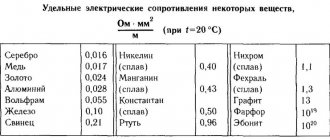
The marking of varistors is different, since each manufacturer of these radio components has the right to install it independently. This is primarily due to its technical characteristics. For example, differences in voltages and required current levels for its operation.
You may be interested in this Description of the electrical circuit diagram with an example
Among domestic ones, the most common is K275, and among imported ones - 7n471k, 14d471k, kl472m and ac472m. The most popular is a varistor, the marking of which is CNR (there are also hel, vdr, jvr). In addition, the alphanumeric index 14d471k is attached to it, and this type of designation is deciphered as follows:
- CNR - metal oxide type.
- 14 - device diameter equal to 14 mm.
- D is a disc-shaped radio component.
- 471 is the maximum voltage value for which it is designed.
- K is the permissible deviation of the classification voltage equal to 10%.
Their main characteristics:
- Classification voltage is the value of the potential difference, taken into account that a current of 1 mA flows through the varistor.
- The maximum value of the alternating voltage is the rms value at which it opens and, therefore, the value of its resistance decreases.
- The constant maximum voltage value at which the varistor opens in a DC circuit. As a rule, it is greater than the previous parameter for a current of variable amplitude.
- The permissible voltage (limitation voltage) is the value above which the element fails. Indicated for a specific current value.
- The maximum energy absorbed is measured in J (joules). This characteristic shows the amount of pulse energy that a varistor can dissipate and not fail.
- Response time (unit - nanoseconds, ns) - the value required to transition from one state to another, that is, a change in resistance value from a high value to a low value.
- Classification voltage error is a deviation from its nominal value in both directions, which is indicated in % (for imported models: K = 10%, L = 15%, M = 20% and P = 25%).
Checking the integrity of the protective diode
Checking the integrity of the protective, as well as the rectifying (including power) diode, is carried out with a multimeter (as an option, you can use an ohmmeter). The device can be used for this purpose only in dialing mode.
Fig 3 Checking the protective diode
When the multimeter is ready, you need to connect it with probes to the suppressor terminals (positive-red with the anode, negative-black with the cathode). When this is done, the display of the testing device will display a number indicating the threshold voltage of the diode fuse being tested. When changing the polarity of the connection, an infinite resistance value should be displayed. If everything turned out this way, then the element is working.
If a leak is detected during a pole change, we can talk about the dysfunction of the element and the need to replace it. Similarly, you can check the protective diode of a car generator.
Basic qualities of TVS diodes
But, as a result, it is necessary to recognize that the fulfillment of one condition often entails a violation of another.
In addition, the TVS diode, in principle, cannot be considered an ideal protective limiter. For example, suppressor protective diodes in the “off” position can be characterized by fairly large reverse currents. Further, abruptness when changing modes is disapproved. The biggest problem is that in the limiting mode the voltage level is directly dependent on the current strength.
It must be remembered that all diode characteristics given by the manufacturer are valid only under specific temperature conditions. At higher temperatures, the permissible peak power and currents will decrease.
Designation, parameters and application of protective diodes
Among the variety of semiconductor devices, diodes are probably the largest family. Schottky diodes, Gunn diodes, zener diodes, LEDs, photodiodes, tunnel diodes and many more different types and applications.
One of the classes of semiconductor diodes in our literature is called SOL (semiconductor voltage limiter) or suppressor. In foreign technical literature the name TVS diode ( Transient Voltage Suppressor is . Very often, TVS diodes are named by manufacturer brands: TRANSIL, INSEL.
In the technical literature and among radio amateurs, a suppressor can be called differently: protective diode, limiting zener diode, TVS diode, transil, voltage limiter, limiting diode. Suppressors can often be found in switching power supplies - there they serve as protection against overvoltage of the powered circuit in the event of faults in the switching power supply.
Let's consider what a TVS diode is, its principle of operation, in what circuits and for what purposes it is used.
TVS diodes were created in 1968 in the USA to protect industrial equipment from atmospheric electricity discharges. In the operating conditions of electronic devices for both industrial and household purposes, great importance is attached to protecting these devices from natural electrical impulses.
Voltage surges also often occur at power transformer substations. In such cases, hundreds of household appliances break down. Because industrial enterprises have comprehensive protection, but residential buildings are not protected at all in this case.
To protect equipment from the effects of electrical overvoltages, a class of semiconductor devices called TVS diodes or “suppressors” was developed. Sometimes in a conversation you can hear: diode fuse.
Designation on the diagram.
On circuit diagrams, the suppressor (aka protective diode) is designated as follows (VD1, VD2 - symmetrical; VD3 - unidirectional).
Operating principle of a suppressor (protective diode).
TVS diodes have a pronounced nonlinear current-voltage characteristic. If the amplitude of the electrical pulse exceeds the rated voltage for a particular type of diode, it will go into avalanche breakdown mode. That is, the TVS diode will limit the voltage pulse to a normal value, and the “excess” goes to the case (ground) through the diode. The process looks more clearly in the figure.
As long as there is no threat of failure of the electronic device, the TVS diode does not have any effect on the operation of the equipment. This semiconductor device is faster than previous limiters.
Safety diodes are available both asymmetrical (unidirectional) and symmetrical (bidirectional). Symmetrical ones can operate in circuits with bipolar voltages, and asymmetrical ones only with voltages of one polarity. Another typical connection diagram (for a bidirectional diode).
For a unidirectional suppressor, the circuit looks a little different.
If the input voltage increases, the device reduces its resistance in a very short time. The current in the circuit increases sharply and the fuse blows. Since the suppressor operates very quickly, there is no harm to the equipment. A distinctive feature of TVS diodes is their very short response time to overvoltage. This is one of the “features” of protective diodes.
Basic electrical parameters of suppressors.
U samples (V) – breakdown voltage value. In foreign technical documentation, this parameter is designated as VBR ( Breakdown Voltage ). This is the voltage value at which the diode suddenly opens and diverts a dangerous current pulse to the common wire (“to ground”).
I arr. (µA) – value of constant reverse current. This is the value of the maximum reverse leakage current that all diodes have. It is very small and has virtually no effect on the operation of the circuit. Another designation is IR ( Max. Reverse Leakage Current ). May also be referred to as IRM.
U arr. (V) – constant reverse voltage. Corresponds to the English abbreviation VRWM ( Working Peak Reverse Voltage ). May be referred to as VRM.
U limit imp. (V) – maximum impulse limiting voltage. In datasheets it is designated as VCL or VC – Max. Clamping Voltage or simply Clamping Voltage .
I ogr. max. (A) – maximum peak pulse current. In English it is designated as IPP ( Max. Peak Pulse Current ). This value shows the maximum value of the current pulse the suppressor can withstand without destruction. For powerful suppressors, this value can reach several hundred amperes!
P imp. (Watt) – maximum permissible pulse power. This parameter shows how much power the suppressor can suppress. Let us recall that the word suppressor comes from the English word Suppressor , which means “suppressor”. Foreign name for the parameter Peak Pulse Power ( PPP ).
The value of the maximum pulse power can be found by multiplying the values of U limit. imp. ( VCL ) and I limit. max. ( IPP ).
The current-voltage characteristics of a symmetrical and asymmetrical TVS diode are as follows.
CVC of a unidirectional protective diode (suppressor) CVC of a bidirectional suppressor
The big disadvantage of these diodes is the large dependence of the maximum pulse power on the pulse duration. Typically, the operation of a TVS diode is considered when a pulse is applied to it with a minimum rise time of about 10 microseconds and a short duration.
For example, with a pulse duration of 50 microseconds, an SMBJ 12A diode can withstand a pulse current that is almost four times the rated one.
Small-sized diodes TRANSZORB TM series 1.5KE6.8 - 1.5KE440 (C)A . They are available in both symmetrical and asymmetrical versions. For a symmetrical diode, the letter C or CA is added to the designation. This series has a wide range of operating voltages from 5.0 to 376 volts, a short response time of 1 * 10-9 sec, and the ability to suppress high-power pulses up to 1500 W. They have proven themselves excellent in protection schemes for television, digital and other modern equipment.
Diodes are available in DO-201 package.
Dimensions are indicated in inches and millimeters (in parentheses). Asymmetrical suppressors have a colored marking ring on the body, which is located closer to the cathode terminal.
The body contains the marking of the protective diode, which encodes its main parameters.
Bidirectional diodes TRANSIL TM 1.5KE440CA are successfully used to protect household electronic equipment in 220 volt networks. Their use is most effective for protecting objects that are connected to overhead lines. In this case, there will be protection both from atmospheric electrical impulses and from impulse overvoltages along power circuits.
TVS diodes TRANSZORB series 1.5KE6.8–1.5KE440CA (1N6267–1N6303A)
Diodes of the 1.5KE6.8–1.5KE440CA series are available in symmetrical and asymmetrical versions. The suffix C or CA is added to the designation of a symmetrical diode. For example, 1.5KE6.8C, 1.5KE440CA. The 1N6267–1N6303A series is available in an asymmetrical version only.
| Dimensional drawing | Diode symbols |
| ppm from td for series of discrete TVS diodes 1.5KE6.8-1.5KE440CA (1N6267-1N6303A) series" title="" width="387″ height="306″> |
| Rice. 6. Dependence of P ppm on td for a series of discrete TVS diodes of the 1.5KE6.8-1.5KE440CA series (1N6267-1N6303A) |
| ppm or I pp from T for series of discrete TVS diodes series 1.5KE6.8 - 1.5KE440CA (1N6267 - 1N6303A)" title="" width="350″ height="351″> |
| Rice. 7. Dependence of P ppm or I pp on T for a series of discrete TVS diodes of the 1.5KE6.8 - 1.5KE440CA (1N6267 - 1N6303A) series |
| (BR) for series of discrete TVS diodes series 1.5KE6.8 - 1.5KE440CA (1N6267 - 1N6303A)" title="" width="350″ height="268″> |
| Rice. 8. Dependence of C on V (BR) for a series of discrete TVS diodes of the 1.5KE6.8 - 1.5KE440CA (1N6267 - 1N6303A) series |
Operating principle of a suppressor (TVS diode)
This protective semiconductor has an interesting nonlinear current-voltage characteristic. If the pulse amplitude exceeds the reference data, it will go into avalanche breakdown mode. That is, the suppressor will limit the electrical impulse to the nominal value, and the excess will flow to the ground through it.
A TVS diode can be asymmetrical or symmetrical. The former are used to operate only in DC networks, because in operating condition they allow current to flow in only one direction. Symmetrical suppressors allow current to flow in both directions and are therefore capable of operating in AC networks. An asymmetrical protective limiter is included in the circuit in the opposite direction when installing conventional diodes, that is, the anode is connected to the negative bus, and the cathode to the positive.
If the input level increases, the protective semiconductor sharply reduces its internal resistance in a very short time. The current in the circuit increases sharply and the fuse blows. Since the suppressor operates almost instantly, the main circuit does not have time to burn out. A distinctive feature of TVS diodes is their very low response time to exceeding the voltage level.
Basic electrical parameters of suppressors
A huge disadvantage of suppressors can be considered the strong dependence of the maximum pulse power on the pulse duration. TVS diodes are available in various power levels. However, if these ratings are not enough, then the power can be increased by connecting several semiconductors in series. So, when two are connected, their total power doubles.
Limiting diodes can also be used as zener diodes. But in order to include TVS diodes in a circuit in this way, it is necessary to check reference data on the values of maximum power dissipation, as well as dynamic resistance under conditions of maximum and minimum possible currents.
Suppressors are characterized by a high rate of performance. Their response time is so short that the “bad” current pulses do not have time to cause damage to the equipment.
Source
Operating principle and device
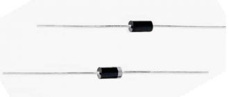
Protection diodes consist of two plates made of germanium or silicon, which have different electrical conductivities. The wire leads of the electrodes are usually soldered to metal layers deposited on the outer surfaces of the plates. The design is enclosed in a plastic, metal-glass or ceramic case.
The operating principle of the protective diode is based on the use of reversible breakdown. As long as the voltage does not exceed the nominal value, the limiter does not have any significant effect on the operation of the circuit, but the device will go into avalanche breakdown mode as soon as the electric pulse amplitude exceeds the base voltage. Thus, the amplitude size is normalized, and all excess voltage goes to the ground through the limiter itself.